CIQTEK Scanning Electron Microscope for MLCC Applications
Ceramic capacitors, as a kind of basic passive components, are an indispensable member of the modern electronic industry. Among them, chip multilayer ceramic capacitors (MLCC) occupy more than 90% of the ceramic capacitor market due to their characteristics of high temperature resistance, high voltage resistance, small size, and wide range of capacitance, and are widely used in the consumer electronics industry, including home appliances, communications, automotive electronics, new energy, industrial control, and other application areas.
The use of CIQTEK SEM can assist in completing the failure analysis of MLCC, finding the origin of failure through micro-morphology, optimizing the production process, and achieving the goal of high product reliability.
Application of CIQTEK SEM in MLCC
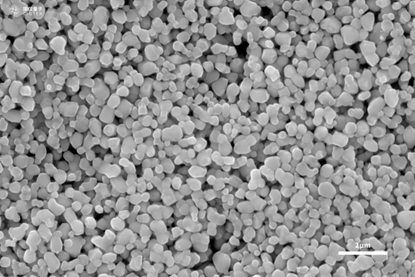
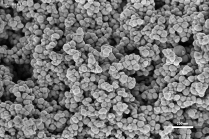
MLCC consists of three parts: inner electrode, ceramic dielectric and end electrode. With the continuous updating of the market demand of electronic products, MLCC product technology also presents the development trend of high capacity, high frequency, high temperature and high voltage resistance, high reliability and miniaturization. Miniaturization means the need to use smaller-sized, more uniform ceramic powders. The microstructure of the material determines the final performance, and the use of scanning electron microscope to characterize the microstructure of ceramic powders, including particle morphology, particle size uniformity, and grain size, can help in the continuous improvement of the preparation process.

Scanning electron microscope imaging of different types of barium titanate ceramic powders /25kV/ETD

Scanning Electron Microscope Imaging Different types of barium titanate ceramic powders /1kV/Inlens
High reliability means that a deeper understanding of the failure mechanism is required, and therefore failure analysis is indispensable. The root cause of MLCC failure is the presence of various microscopic defects, such as cracks, holes, delamination, etc., either externally or internally. These defects will directly affect the electrical performance and reliability of MLCC products, and bring serious hidden danger to product quality. The use of scanning electron microscope can assist in completing the failure analysis of capacitor products, find the origin of the failure through the microscopic morphology, optimize the production process, and ultimately achieve the goal of high reliability of the product.
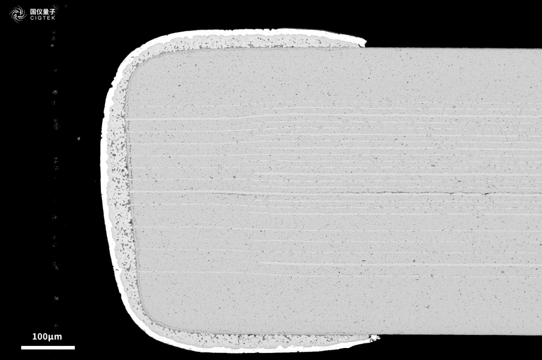
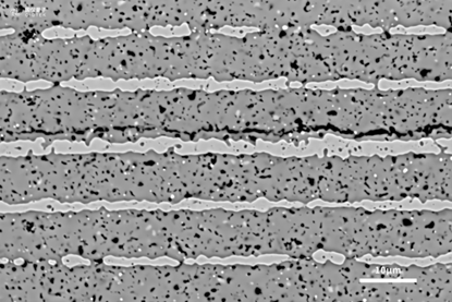
MLCC's internal is a multi-layer structure, each layer of ceramics whether there are defects, multi-layer ceramics thickness is uniform, whether the electrodes are covered uniformly, all of these will affect the life of the device. When using SEM to observe the internal multilayer structure of MLCC or to analyze their internal failures, it is often necessary to perform a series of pre-treatments on the samples before they can be tested. These include resin embedding, mechanical grinding, conductive treatment by a coater, etc. Further finishing treatment can also be done using an ion mill. The figure below shows the microscopic morphology of the internal cross-section of the MLCC taken with a CIQTEK tungsten filament SEM3200. As seen in the figure, delamination of the ceramic dielectric layer may be the cause of device failure.

MLCC Section/15kV/BSED

MLCC Section/20kV/BSED
In recent years, the demand for MLCC has seen a new round of growth with the booming development of consumer electronics, communication equipment and automotive industries. The use of CIQTEK SEM to characterize the relevant morphology and compositional homogeneity of MLCC will help MLCC manufacturers to sustain the development of high reliability.

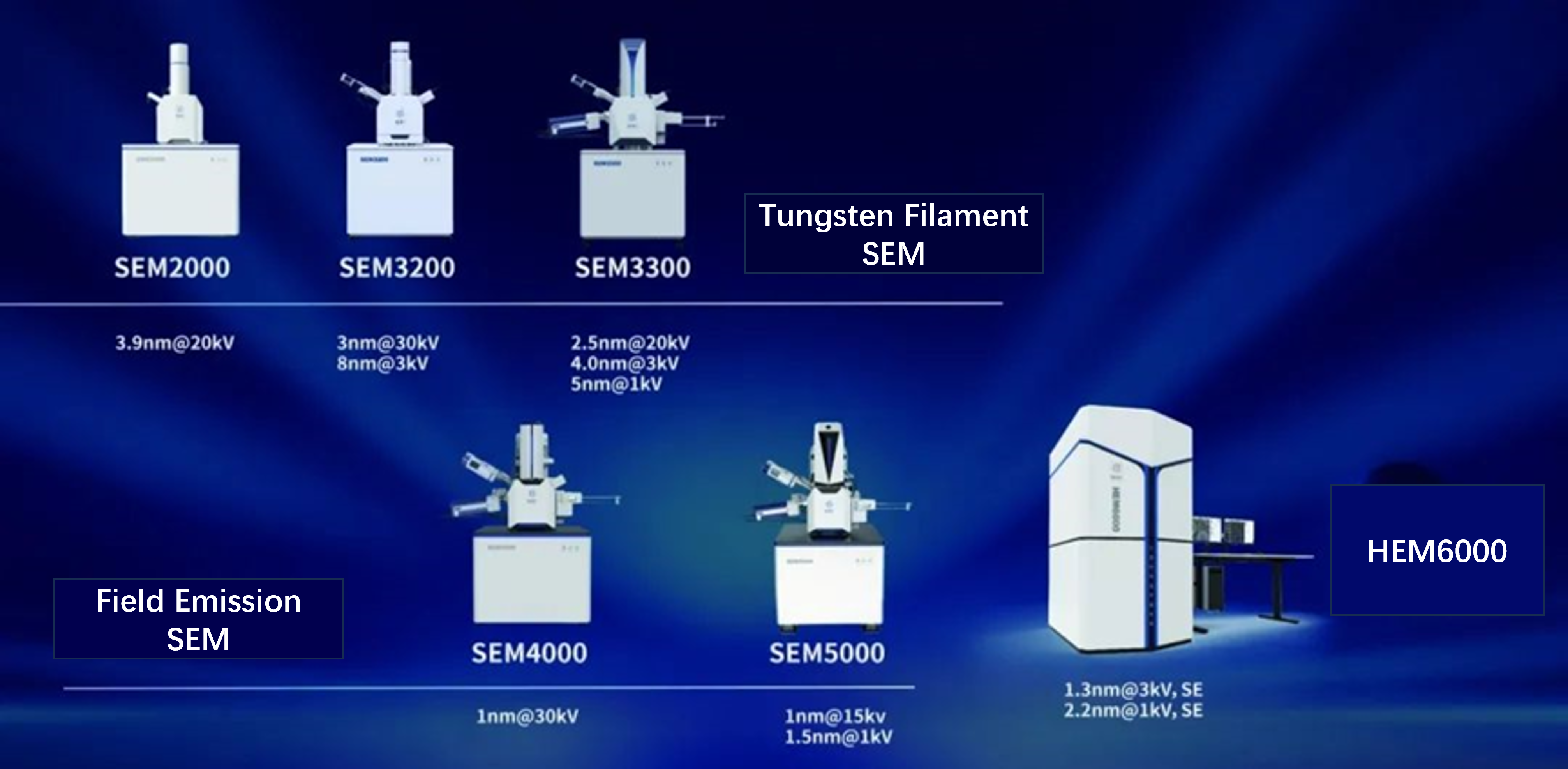
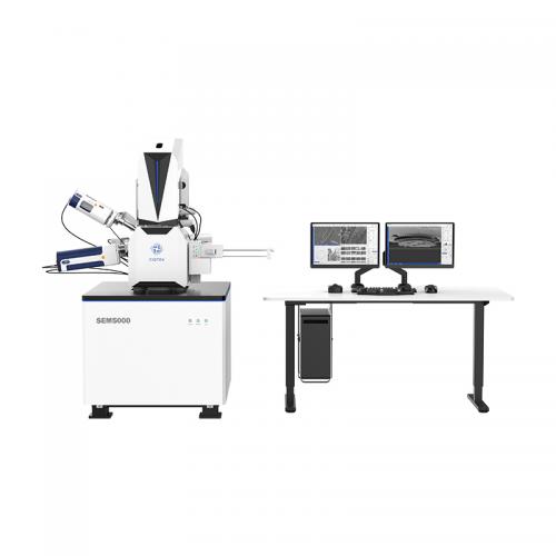
CIQTEK SEM5000 is a field emission scanning electron microscope(FESEM) with high-resolution imaging and analysis ability, supported by abundant functions, benefits from advanced electron optics column design, with high-pressure electron beam tunnel technology (SuperTunnel), low aberration, and non-immersion objective lens, achieves low voltage high-resolution imaging, the magnetic specimen can also be analyzed. With optical navigation, automated functionalities, carefully designed human-computer interaction user interface, and optimized operation and use process, no matter if you are an expert or not, you can quickly get started and complete high-resolution imaging and analysis work.
Learn More
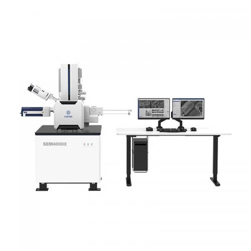
High-Performance and Multi-Purpose Field Emission Scanning Electron Microscope The SEM4000X (G2) is an ideal FE-SEM for microscale analysis and inspection. Combining stable, user-friendly operation with a multi-detector system and beam-deceleration capabilities, it delivers high-resolution imaging at low landing voltages. Balancing performance, reliability, and total cost of ownership, it provides a dependable solution for modern materials-analysis laboratories.
Learn More
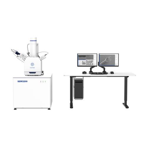
High-Performance and Universal Tungsten Filament SEM Microscope The CIQTEK SEM3200 SEM Microscope is an excellent general-purpose Tungsten Filament Scanning Electron Microscope (SEM) with outstanding overall capabilities. Its unique Dual-anode electron gun structure ensures high resolution and improves image signal-to-noise ratio at low excitation voltages. Furthermore, it offers a wide range of optional accessories, making the SEM3200 a versatile analytical instrument with excellent expandability. Contact our U.S. team: info.usa@ciqtek.com
Learn More
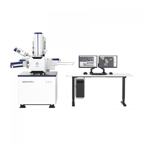
Analytical Schottky Field Emission Scanning Electron Microscope (FESEM) CIQTEK SEM4000Pro is an analytical FE-SEM model equipped with a high-brightness and long-life Schottky field emission electron gun. Its three-stage electromagnetic lens design offers significant advantages in analytical applications such as EDS / EDX, EBSD, WDS, and more. The model comes standard with a low-vacuum mode and a high-performance low-vacuum secondary electron detector, as well as a retractable backscattered electron detector, which benefits the observation of poorly conductive or non-conductive specimens. Contact our U.S. team: info.usa@ciqtek.com
Learn More
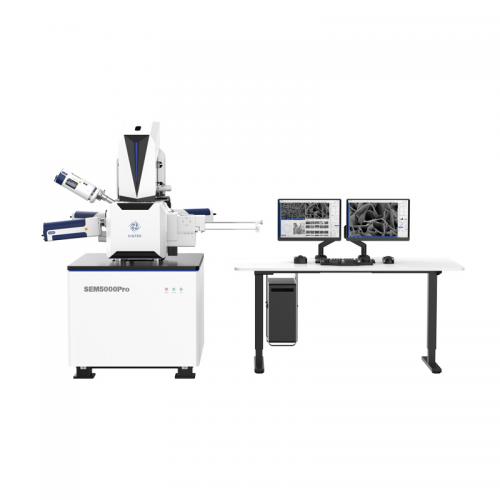
Ultra-High Resolution Schottky Field Emission Scanning Electron Microscope The SEM5000Pro (G2) field-emission scanning electron microscope is designed for stability, reliability, ease of use, and productivity, bringing field-emission imaging capabilities to a wide range of laboratories. Combining ultra-high spatial resolution with long-term operating stability, it consistently delivers high-quality images for applications ranging from advanced nanomaterials characterization to semiconductor R&D and manufacturing, meeting the demanding needs of research institutions and industrial quality-control laboratories.
Learn More
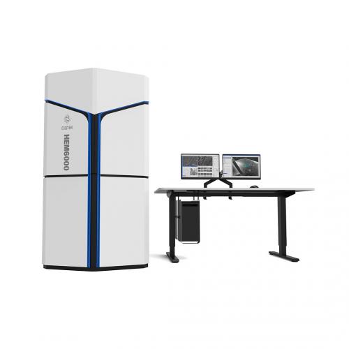
High-speed Fully Automated Field Emission Scanning Electron Microscope Workstation CIQTEK HEM6000 facilities technologies such as the high-brightness large-beam current electron gun, high-speed electron beam deflection system, high-voltage sample stage deceleration, dynamic optical axis, and immersion electromagnetic & electrostatic combo objective lens to achieve high-speed image acquisition whilst ensuring nano-scale resolution. The automated operation process is designed for applications such as a more efficient and smarter large-area high-resolution imaging workflow. Its imaging speed is over five times faster than that of a conventional field emission scanning electron microscope (FESEM).
Learn More
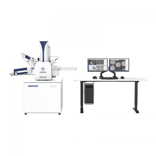
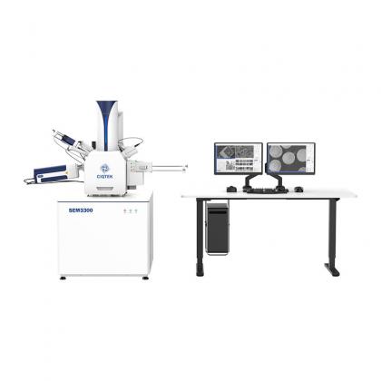
Ultra High-Resolution Tungsten Filament Scanning Electron Microscope The CIQTEK SEM3300 Scanning Electron Microscope (SEM) incorporates technologies such as "Super-Tunnel" electron optics, inlens electron detectors, and electrostatic & electromagnetic compound objective lens. By applying these technologies to the tungsten filament microscope, the long-standing resolution limit of such SEM is surpassed, enabling the tungsten filament SEM to perform low-voltage analysis tasks previously only achievable with field emission SEMs.
Learn More
120kV Field Emission Transmission Electron Microscope (TEM) 1. Divided Workspaces: Users operate TEM in a divided room with comfort reducing environmental interference to TEM. 2. High Operational Efficiency: Designated software integrates highly automated processes, allowing efficient TEM interaction with real-time monitoring. 3. Upgraded Operational Experience: Equipped with a field emission electron gun with a highly automated system. 4. High Expandability: There are sufficient interfaces reserved for users to upgrade to a higher configuration, which meets diverse application requirements.
Learn More
Analytical Schottky Field Emission Scanning Electron Microscopy (FESEM) The SEM5000XLV combines high-resolution imaging with high-current analytical capability and supports rapid switching between low-vacuum and high-current operating modes. It supports integration with optional EDS and EBSD modules, providing efficient characterization of challenging specimens and a comprehensive solution for localized microstructural and compositional analysis. Contact our U.S. team: info.usa@ciqtek.com
Learn More
No. 1969, Kongquetai Road, High-tech Zone, Hefei, Anhui, China
+8615156059133
+8613083191369
info@ciqtek.com
Sitemap | XML | Blog | Privacy Policy | IPv6 network supported