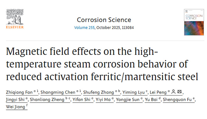
Corrosion Science Spotlight: CIQTEK SEM in Steam Oxide Film Analysis
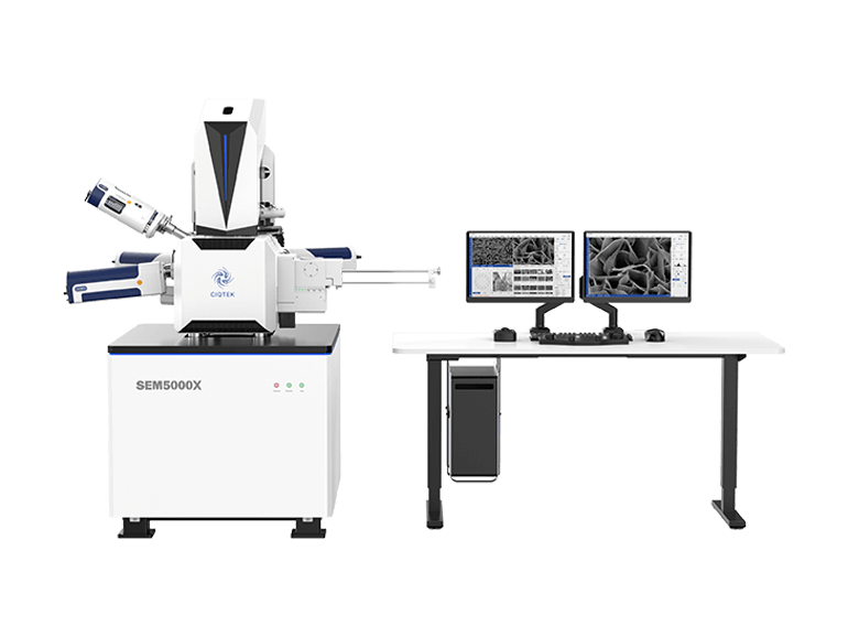
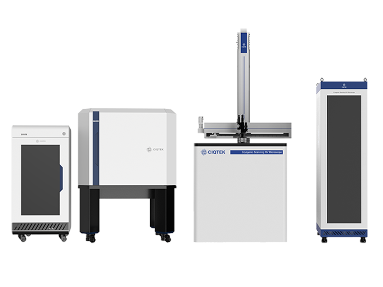
Nuclear fusion is considered a key future energy source due to its high efficiency and clean energy output. In fusion reactors, water cooling systems are widely used because they are technically mature, cost-effective, and have excellent cooling performance. However, a major challenge remains: under high temperature and high pressure, water and steam strongly corrode structural materials. While this problem has been studied in fission reactors, fusion environments are more complex. The unique high-intensity, unevenly distributed magnetic fields in fusion devices interact with corrosion processes, creating new technical challenges that need detailed research. To address this, Associate Professor Peng Lei's team from the University of Science and Technology of China conducted an in-depth study using the CIQTEK scanning electron microscope (SEM) and dual-beam electron microscope. They built high-temperature magnetic-field steam corrosion and high-temperature water corrosion setups. Using SEM, EBSD, and FIB techniques, they analyzed oxide films formed on CLF-1 steel after 0–300 hours of steam corrosion at 400°C under 0T, 0.28T, and 0.46T magnetic fields, and after 1000 hours of high-temperature water corrosion at 300°C. The study used CIQTEK SEM5000X ultra-high-resolution field-emission SEM and the FIB-SEM DB500 The study found that the oxide films form a multilayer structure, with a chromium-rich inner layer and an iron-rich outer layer. Film formation occurs in five stages: initial oxide particles, then floc-like structures, formation of a dense layer, growth of spinel structures on the dense layer, and finally, spinel cracking into laminated oxides. The presence of a magnetic field significantly accelerates corrosion, promotes the transformation of outer magnetite (Fe₃O₄) into hematite (Fe₂O₃), and enhances laminated oxide formation. This work was published in Corrosion Science, a top-tier journal in the field of corrosion and materials degradation, under the title: "Magnetic field effects on the high-temperature steam corrosion behavior of reduced activation ferritic/martensitic steel." Surface Oxide Film Characterization In high-temperature steam (HTS), CLF-1 steel surfaces show different corrosion states over time. On polished surfaces, early-stage oxidation (60 h) appears as small, dispersed particles. The Fe/Cr ratio is similar to the substrate, indicating that the oxide layer is not yet complete. By 120 h, floc-like oxides appear. At 200 h, a dense oxide layer forms, with new oxide particles and local spinel structures on top. Rough surfaces corrode faster. Early floc-like oxides are finer and more evenly distributed. By 200 h, they transform into spinel structures, showing a stronger difference from polished surfaces. In high-temperature, high-pressure water (HTPW), polished surfaces display similar spinel structures. Spinel in HTPW is denser and more numerous, while spinel in HTS is larger in size....