CIQTEK EPR
Product Center

Products

Science & Technology
Science and technology are areas of research and application involving systematic knowledge of the physical and natural world and the practical application of that knowledge. Science is concerned with understanding the fundamental principles and laws of the universe, and technology is concerned with the development and application of tools, machines and techniques to solve practical problems and improve human life.
Materials Science
Materials Science
Using advanced analytical instruments, study the interrelationship between the preparation or processing process of materials, the microstructure of materials, and the macroscopic properties of materials.
Chemicals
Chemicals
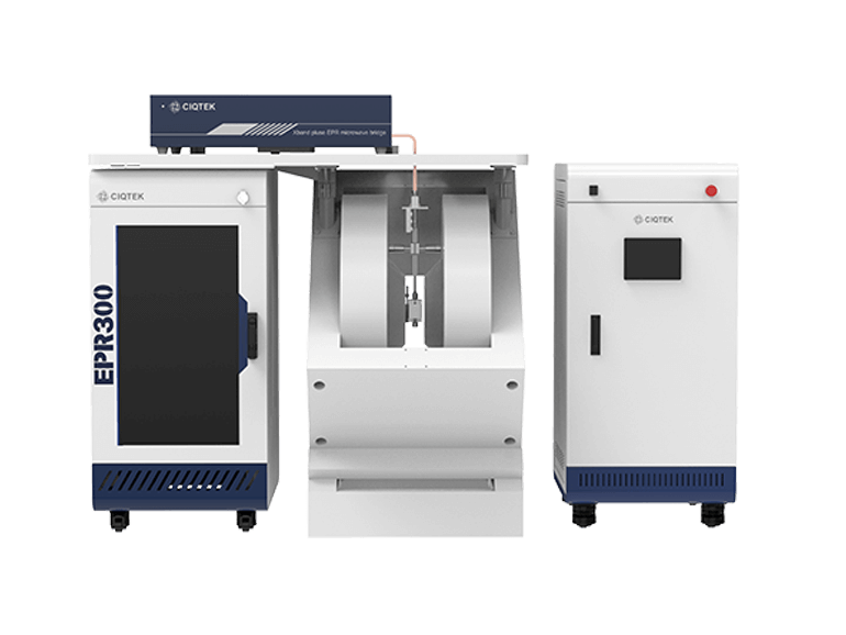
Analysis of the structure of substances containing unpaired electrons (such as isolated single atoms, conductors, magnetic molecules, transition metal ions, rare earth ions, ion clusters, doped materials, defective materials, biological radicals, metalloproteins, etc.) and their applications are realized by using wave spectroscopy.
Industrial & Applied Sciences
Provide high quality, high standard products & solutions for industrial users and applied scientific research based on advanced technology and reliable products.
Energy & Power
Energy & Power
Focus on the utilization of unconventional oil and gas resources such as shale oil and gas, coalbed methane, combustible ice, etc., and develop application scenarios such as downhole digital core analysis.
Biomedical & Life Science
Apply to resolve the structure and function of biological macromolecules, single-molecule imaging, subcellular imaging, cell sorting, and other fields, the measurement scale spans the nanometer to the micron scale.

About CIQTEK

CIQTEK is the global developer & manufacturer of high-value scientific instruments. Our main business includes Electron Microscopes (SEM/FIB, TEM), Nuclear Magnetic Resonance (NMR) Spectrometer, Electron Paramagnetic Resonance (Electron Spin Resonance) Spectrometer, and BET Surface Area & Pore Analyzer.
  • 0+
    Employees
  • 0% +
    Employees dedicated to R&D
  • 0+
    Patents pending or granted
News & Events

News

What's New
CIQTEK Lists on Shanghai STAR Market, Stock Code 688828
CIQTEK Lists on the Shanghai STAR Market CIQTEK held its listing ceremony at the Shanghai Stock Exchange on August 11, 2026. The listing marks a new stage for the company as it continues to develop high-end scientific instruments. The company trades under stock code 688828 and develops, manufactures, and sells products including electron microscopes, electron paramagnetic resonance spectrometers, and nuclear magnetic resonance spectrometers. Listing Information CIQTEK issued 40.0100 million shares at RMB 21.22 per share. The gross proceeds from the new share offering were RMB 849.0122 million. Following the offering, the company had 400.0100 million shares outstanding. In 2025, CIQTEK reported revenue of RMB 666.191845 million. The company is based in Hefei, Anhui Province.   From Research to Real-World Use CIQTEK focuses on turning research capabilities into instruments that can be used in laboratories and industrial settings. At the ceremony, Dr. He Yu, Chairman of CIQTEK, said the listing is an important milestone and a stage in the company’s journey from the laboratory to real-world use. Dr. He thanked customers, partners, investors, and the teams that supported the offering and listing process. A Focus on Useful, Reliable Instruments CIQTEK develops high-end scientific instruments across several product areas. The company continues to invest in research and development and to expand its product portfolio around customer needs. Dr. He said that customer feedback, technical problem-solving, and reliable delivery are central to the company’s long-term improvement. CIQTEK will continue to advance projects funded by the offering and strengthen transparent, standardized governance. Looking Ahead Dr. He noted that better measurement tools support scientific discovery and that high-quality data remains essential as artificial intelligence changes the way research is done. CIQTEK will continue to build instruments for researchers and industrial users around the world. “We will stay focused, keep improving over the long term, and move forward steadily,” Dr. He said in closing.   Reprint Note The opening and “Listing Information” sections are reprinted from a Shanghai Stock Exchange public release. The remaining sections are adapted from an original address by Dr. He Yu, Chairman of CIQTEK, delivered at the listing ceremony.
August 14, 2026

CIQTEK DB550 FIB-SEM Prepares 5nm Chip Samples for TEM Analysis
The CIQTEK DB550 dual-beam FIB-SEM brings together high-resolution electron imaging and precision ion beam processing on a single platform. CIQTEK has validated its DB550 Focused Ion Beam Scanning Electron Microscope (FIB-SEM) on real 5nm process node chip samples, demonstrating production-ready TEM sample preparation with intact fin structures, zero amorphization, and clearly resolved film layers. The results confirm that the DB550 meets the exacting demands of advanced semiconductor failure analysis labs working at the cutting edge of process technology. In advanced chip research and manufacturing, two tools matter above all others. The Transmission Electron Microscope (TEM) lets you see structures at the atomic scale. But before you can look, you need a sample thin enough for electrons to pass through. That is where the dual-beam FIB-SEM comes in. It is the precision workshop that prepares those ultra-thin specimens. Meet the DB550: One Platform for Imaging and Nanoscale Processing The CIQTEK DB550 FIB-SEM integrates two powerful capabilities onto a single platform. On one side, a scanning electron microscope (SEM) delivers high-resolution surface imaging. On the other, a focused ion beam (FIB) performs nanoscale material removal with surgical precision. Together, they bridge the gap between observation and fabrication at dimensions measured in billionths of a meter. At the heart of the DB550 sits a low-voltage, high-resolution electron column paired with CIQTEK's proprietary "Chengying" ion column, developed entirely in-house. The Chengying column is the engine behind the system's nanoscale cutting and etching capabilities. CIQTEK controls the full design and manufacturing pipeline for this critical component. The 5nm Challenge: Why Sample Preparation Gets Harder at Every Node At 5nm and below, chip architectures rely on fin-type field-effect transistors (FinFETs) with fin widths and pitches measured in just a few nanometers. The DB550 is designed to handle the full sample preparation workflow for these demanding process nodes. It starts with high-current rough cutting to quickly remove bulk material and reach the target region. Then it transitions to low-voltage fine polishing to thin the sample to TEM-ready dimensions without damaging the delicate structures underneath. TEM Validation: The Proof Is in the Image CIQTEK prepared a 5nm process node chip sample on the DB550 and transferred it to a TEM for characterization. The results speak for themselves. TEM characterization of a 5nm chip sample prepared on the DB550 shows intact fin structures with clear, well-defined film layers and no amorphization damage. The TEM images revealed that the fin structures remained completely intact after FIB preparation. There was no detectable amorphization in the silicon crystal lattice. The individual film layers appeared clear and sharply defined in the TEM cross-section. These results validate the dual-beam sample preparation performance of the DB550 on...
May 27, 2026

SEM and FIB: A Powerful Combo for PCB Failure Analysis
  A Winning Team: SEM + FIB, the "Golden Combination"   CIQTEK brings SEM and FIB together as a powerful team, providing critical support for PCB process optimization, reliability verification, and root cause determination of failures. SEM High-Resolution Imaging: The "Microscope" for Surface Details The SEM uses a high-resolution electron beam to capture crisp images of PCB surface morphology. It reveals solder pad plating, intermetallic compounds, micro-cracks, tin whiskers, and foreign particle contamination with exceptional clarity. Coupled with energy-dispersive X-ray spectroscopy (EDS), the SEM also performs elemental analysis on microscopic regions. This combination lets engineers identify the chemical signature of defects, making it straightforward to spot issues like short circuits, open circuits, corrosion, and plating anomalies. FIB Nanoscale Cutting: The "Scalpel" for Internal Structures While the SEM excels at surface imaging, the FIB takes over when you need to see what is happening inside the board. Using a nanometer-precision ion beam, the FIB performs targeted cross-sectioning at the exact defect location. It prepares ultra-thin slices through multi-layer boards, blind vias, and buried vias, exposing internal structures that mechanical sectioning simply cannot reach. Think of the FIB as a microscopic surgical tool. It removes material with nanometer accuracy, leaving a clean cross-section ready for imaging and analysis.   CIQTEK Semiconductor Showcase: See It in Action   The Beauty of the Microscopic World, Revealed in Every Detail. Here are real examples of CIQTEK electron microscopes in PCB cross-section observation: Solder Joint Interface Panorama Low magnification observation of capacitor overall morphology, viewing the real microscopic structure of the capacitor solder joint interface from the inside IMC Layer Evaluation Evaluating interlayer bonding, measuring IMC thickness and uniformity, detecting voids, cracks, and interface defects Multi-Layer Board Inner Structure Clear observation of IMC layer morphology, thickness, continuity, and density at the solder pad and solder interface Process Reliability Evaluation Evaluating trace pattern, thickness, etching quality and copper-to-substrate bonding, detecting line shift, etch defects, delamination, voids, and analyzing plating layer quality for PCB process control and reliability assessment   Built for Labs That Demand Reliability   CIQTEK develops its electron microscopy platforms from the ground up, covering core algorithms through hardware design. This vertical integration ensures consistent performance and long-term supply stability, which matters for labs running continuous production or multi-year research programs. The company backs its instruments with responsive technical support and regular software updates, helping users keep their systems running efficiently over time.   Get in Touch If you are evaluating SEM or FIB systems for ...
May 25, 2026

Conferences & Exhibitions
CONTACT US

Contact

Top

Leave A Message

Leave A Message
Please feel free to contact us for more details, request a quote or book an online demo! We will reply you as soon as we can.
Submit

Home

Products

Chat

contact