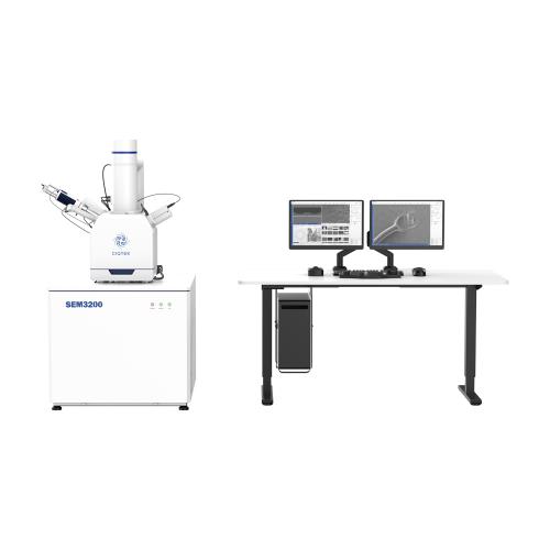
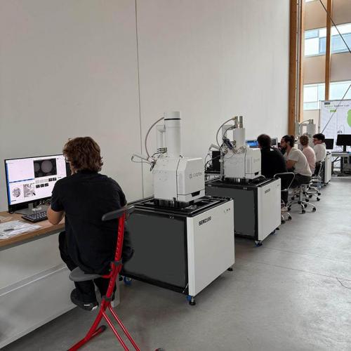
sem microscope for sale

Tungsten Filament SEM | SEM2100

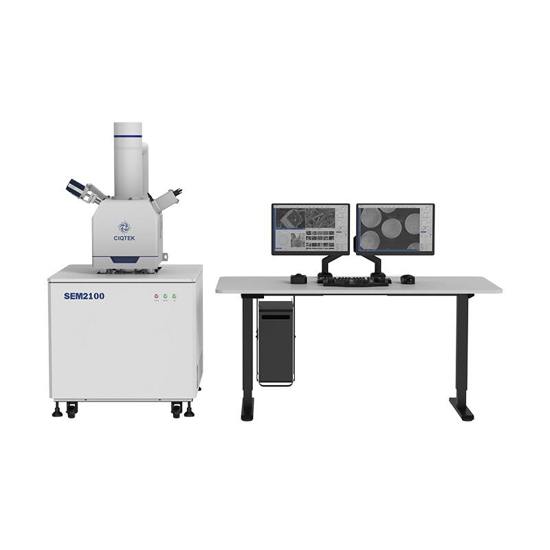
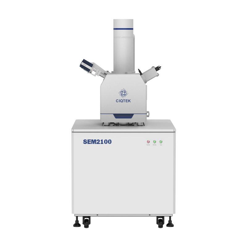
Easy-to-Use Compact Tungsten Filament Scanning Electron Microscope


The CIQTEK SEM2100 SEM Microscope features a simplified operating process and adheres to industry standards and user habits in its "User Interface" design. Despite the minimalist software interface, it provides comprehensive automated functions, measurement and annotation tools, image post-processing management capabilities, optical image navigation, and more. The design of SEM2100 perfectly realizes the idea of "Simplicity without sacrificing functionality".

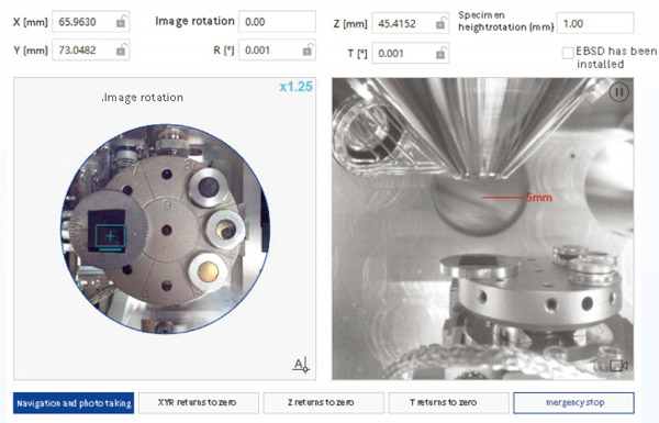
Optical Navigation

Using a vertically mounted chamber camera to capture optical images for specimen stage navigation allows for a more intuitive and accurate specimen positioning.

  • SEM Optical Navigation

▶Intelligent Assisted Image Astigmatism Correction

Under this mode, the astigmatism value of X and Y varies with the pixels. The image clarity is maximized at the optimal astigmatism value, enabling rapid stigmator adjustment.

  • sem Intelligent Assisted Image Astigmatism Correction
  • sem Intelligent Assisted Image Astigmatism Correction


Auto Functions

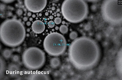
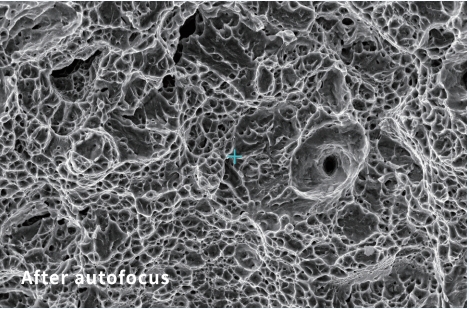
Improved Automatic Brightness & Contrast, Automatic Focus, and Automatic Astigmatism Correction Functions. Imaging by a single click!

>> Automatic Focus

  • during autofocus
  • after autofocus


>> Automatic Astigmatism Correction

  • during autofocus
  • after autofocus


>> Automatic Brightness & Contrast

  • during autofocus
  • after autofocus

Safer to Use


Easy Filament Replacement

Pre-aligned replacement filament module ready to use.


Particle & Pore Analysis Software (Particle) *Optional

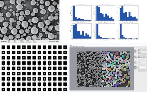
SEM Particle & Pore Analysis Software (Particle)

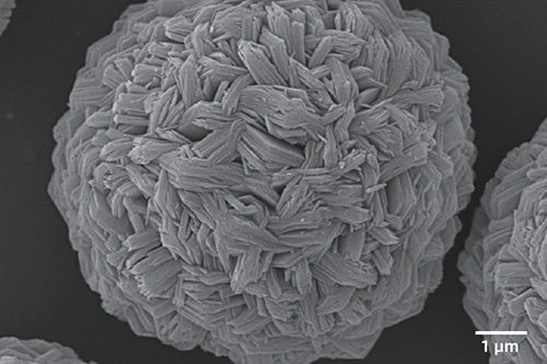
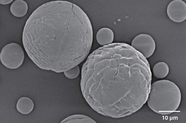
The CIQTEK SEM Microscope software employs various target detection and segmentation algorithms, suitable for different types of particle and pore samples. it enables quantitative analysis of particle and pore statistics and can be applied in fields such as materials science, geology, and environmental science.


Image Post-processing Software

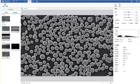
SEM Microscope Image Post-processing Software

Perform online or offline image post-processing on images captured by electron microscopes and integrate commonly used EM image processing functions, convenient measurement, and annotation tools.


Auto Measure *Optional

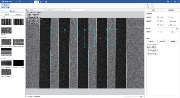
SEM Microscope software Auto Measure

Automatic recognition of line width edges, resulting in more accurate measurements and higher consistency. Support multiple edge detection modes, such as Line, Space, Pitch, etc. Compatible with multiple image formats and equipped with various commonly used image post-processing functions. The software is easy to use, efficient, and accurate.


Software Development Kit (SDK) *Optional

SEM Microscope Software Development Kit (SDK)

Provide a set of interfaces for controlling the SEM microscope, including image acquisition, operating condition settings, power on/off, stage control, etc. Concise interface definitions allow for the rapid development of specific electron microscope operation scripts and software, enabling automated tracking of regions of interest, industrial automation data acquisition, image drift correction, and other functions. Can be used for software development in specialized areas such as diatom analysis, steel impurity inspection, cleanliness analysis, raw material control, etc.


AutoMap *Optional

  • during autofocus


CIQTEK SEM2100 SEM Microscope
Electron Optics Resolution 3 nm @ 20 kV, SE
4 nm @ 20 kV, BSE
Accelerating Voltage 0.2 kV ~ 30 kV
Magnification (Polaroid) 1 x ~ 300,000 x
Specimen Chamber Camera Optical Navigation
Chamber Monitoring
Stage Type 3-Axis, XYZ Axis Vacuum Compatible Motorized
XY Range 125 mm
Z Range 50 mm
SEM Detectors Standard Everhart-Thornley Detector (ETD)
Optional Retractable Back-Scattered Electron Detector (BSED)
Energy Dispersive Spectrometer (EDS / EDX)
Electron Backscattered Diffraction Pattern (EBSD)
Optional Specimen Exchange Loadlock
Trackball & Knob Control Panel
User Interface Operating System Windows
Navigation Optical Navigation, Gesture Quick Navigation, Trackball (Optional)
Automatic Functions Auto Brightness & Contrast, Auto Focus, Automatic Stigmator
Leave A Message
Please feel free to contact us for more details, request a quote or book an online demo! We will reply you as soon as we can.
Submit
Related Products
fib sem microscopy

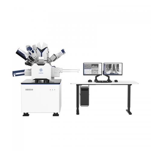
Ga+ Focused Ion Beam Field Emission Scanning Electron Microscope   The CIQTEK DB550 Focused Ion Beam Scanning Electron Microscope (FIB-SEM) has a focused ion beam column for nano-analysis and specimen preparation. It utilizes “super tunnel” electron optics technology, low aberration, and non-magnetic objective design, and has the “low voltage, high resolution” feature to ensure its nanoscale analytical capabilities.   The ion columns facilitate a Ga+ liquid metal ion source with highly stable and high-quality ion beams to ensure nanofabrication capabilities. The DB550 is an all-in-one nano-analysis and fabrication workstation with an integrated nano-manipulator, gas injection system, and user-friendly GUI software.

Learn More
sem electron microscope

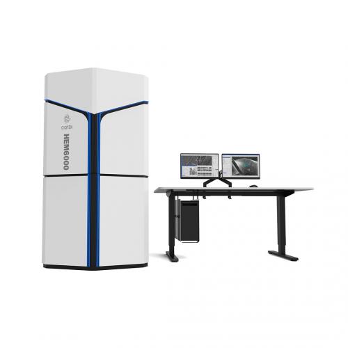
High-speed Fully Automated Field Emission Scanning Electron Microscope Workstation   CIQTEK HEM6000 facilities technologies such as the high-brightness large-beam current electron gun, high-speed electron beam deflection system, high-voltage sample stage deceleration, dynamic optical axis, and immersion electromagnetic & electrostatic combo objective lens to achieve high-speed image acquisition whilst ensuring nano-scale resolution. The automated operation process is designed for applications such as a more efficient and smarter large-area high-resolution imaging workflow. Its imaging speed is over five times faster than that of a conventional field emission scanning electron microscope (FESEM).

Learn More
FESEM EDX

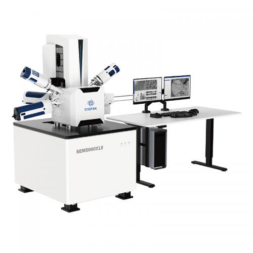
Analytical Schottky Field Emission Scanning Electron Microscopy (FESEM)   The SEM5000XLV combines high-resolution imaging with high-current analytical capability and supports rapid switching between low-vacuum and high-current operating modes. It supports integration with optional EDS and EBSD modules, providing efficient characterization of challenging specimens and a comprehensive solution for localized microstructural and compositional analysis.     Contact our U.S. team: info.usa@ciqtek.com

Learn More
field emission scanning electron microscopy

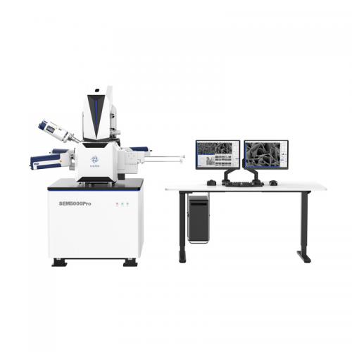
Ultra-High Resolution Schottky  Field Emission Scanning Electron Microscope The SEM5000Pro (G2) field-emission scanning electron microscope is designed for stability, reliability, ease of use, and productivity, bringing field-emission imaging capabilities to a wide range of laboratories. Combining ultra-high spatial resolution with long-term operating stability, it consistently delivers high-quality images for applications ranging from advanced nanomaterials characterization to semiconductor R&D and manufacturing, meeting the demanding needs of research institutions and industrial quality-control laboratories.  

Learn More
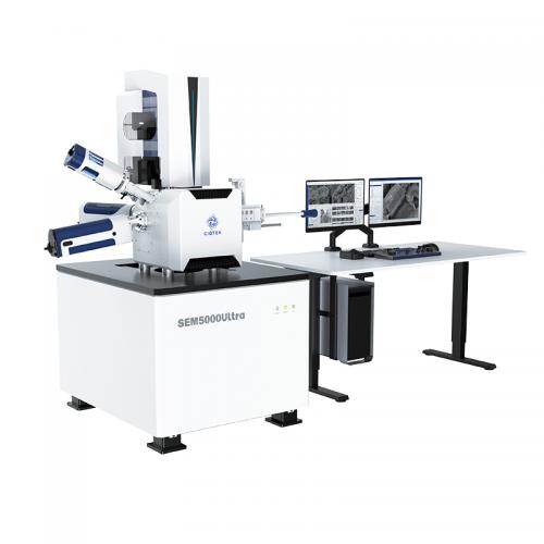
Ultra-High Resolution Schottky FESEM | SEM5000Ultra

Versatile Performance, One-Click Imaging Engineered for Challenging Specimens   Combining ultra-high spatial resolution with high-current analytical capability at low landing energies, it is designed for challenging samples. With excellent resolution across the full voltage range, it supports rapid high-resolution analysis at large beam current. From sample loading to image output, one click delivers simple, efficient, and high-definition imaging of critical samples for frontier research and high-end semiconductor applications.  

Learn More
field emission sem price

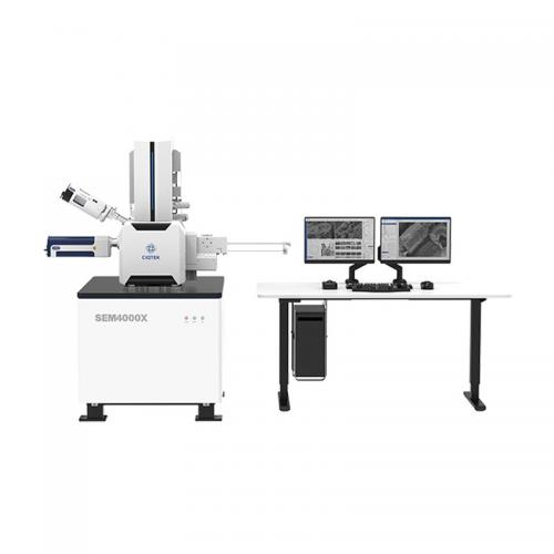
High-Performance and Multi-Purpose Field Emission Scanning Electron Microscope   The SEM4000X (G2) is an ideal FE-SEM for microscale analysis and inspection. Combining stable, user-friendly  operation with a multi-detector system and beam-deceleration capabilities, it delivers high-resolution imaging at low landing voltages. Balancing performance, reliability, and total cost of ownership, it provides a dependable solution for modern materials-analysis laboratories.  

Learn More
scanning electron microscope machine

High-Performance and Universal Tungsten Filament SEM Microscope   The CIQTEK SEM3200 SEM Microscope is an excellent general-purpose Tungsten Filament Scanning Electron Microscope (SEM) with outstanding overall capabilities. Its unique Dual-anode electron gun structure ensures high resolution and improves image signal-to-noise ratio at low excitation voltages. Furthermore, it offers a wide range of optional accessories, making the SEM3200 a versatile analytical instrument with excellent expandability.   Contact our U.S. team: info.usa@ciqtek.com

Learn More
sem microscope price

Read the CIQTEK SEM Microscopes customer insights and learn more about CIQTEK's strengths and achievements as the SEM industry leader!   Email: info@ciqtek.com

Learn More
Top

Leave A Message

Leave A Message
Please feel free to contact us for more details, request a quote or book an online demo! We will reply you as soon as we can.
Submit

Home

Products

Chat

contact