CIQTEK Scanning Electron Microscope Facilitates Research on Advanced Energy Storage Materials
August 08, 2023
Energy storage is considered to be the last step in the development of new energy, and is the key to whether new energy can play a major role and whether it can realize the goal of "carbon neutrality".
As a new type of energy storage technology, supercapacitors, with high power density, low temperature, long cycle life, wide operating temperature range, and other characteristics, can be widely used in new energy vehicles, wind power, photovoltaic power generation, as well as consumer electronics, has attracted much attention in recent years. To further improve the performance of supercapacitors, in addition to the existing technology, but also to consider the development of new technologies and new materials, the Shandong Advanced Electromagnetic Drive Technology Research Institute of Researchers Sun has deep and extensive research on this.
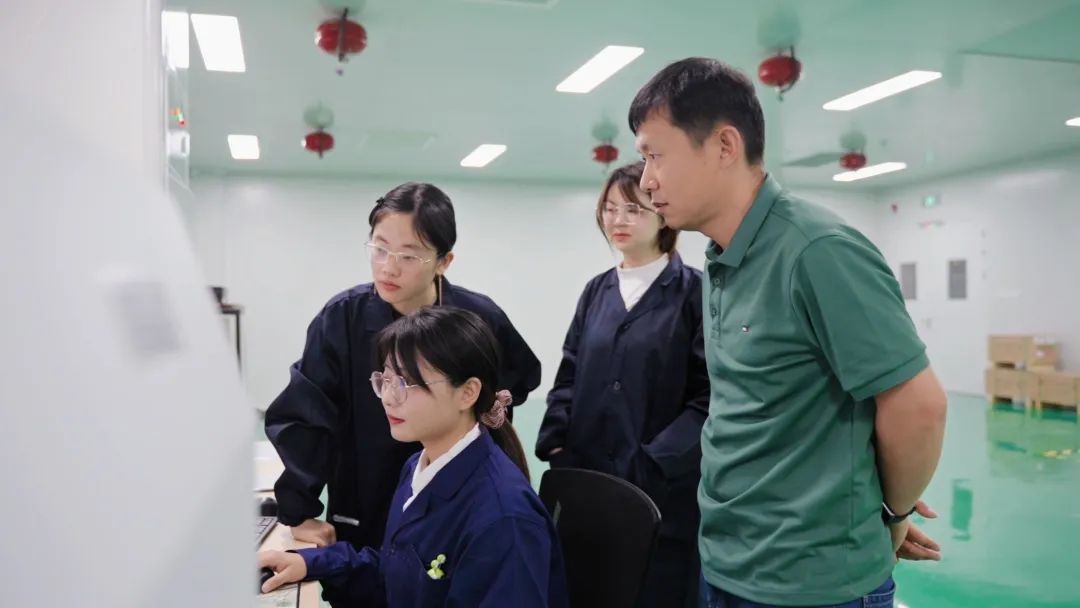
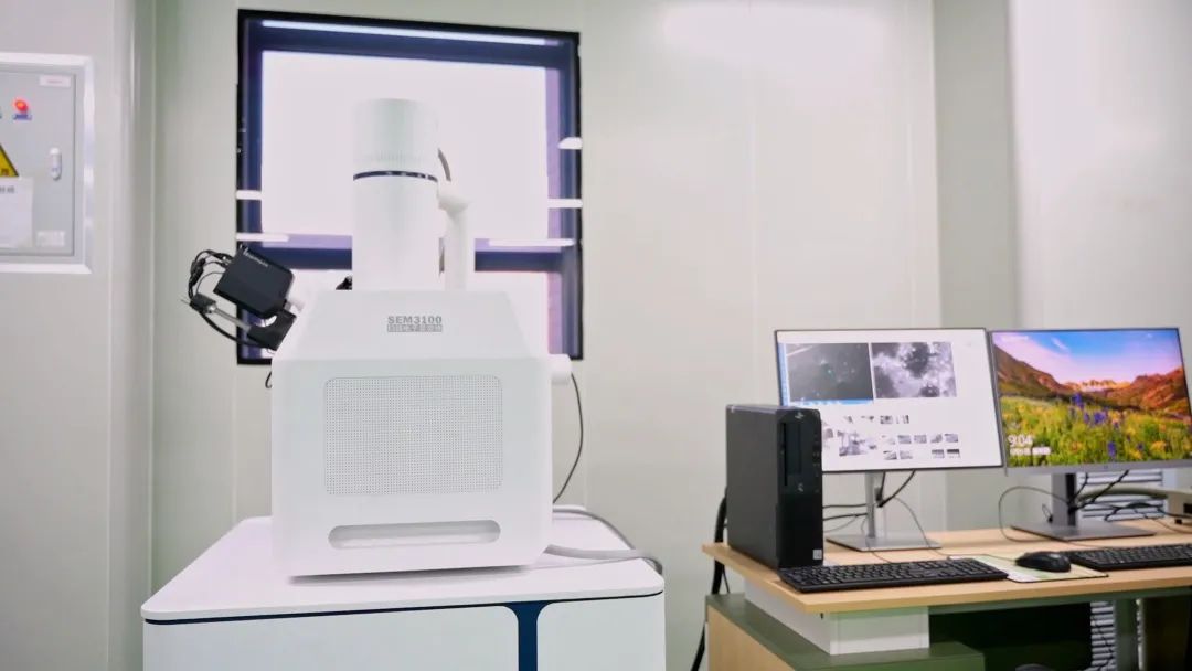
To meet the demand for research on various types of energy storage materials, the group of researcher Sun introduced in October 2021 a tungsten filament scanning electron microscope (SEM) independently developed by CIQTEK. It is understood that scanning electron microscopy is an important research tool in materials science, which is mainly applied in the study of material structure, morphology, composition, properties, and failure analysis. At present, the materials tested by the Institute using the CIQTEK SEM include activated carbon, metal oxides, soft carbon, hard carbon, and other electrode materials. At the same time, the group also uses SEM to analyze the causes of failure of supercapacitors and battery monomers.
"The previous electron microscope required taking a picture with a cell phone to remember the sample location before selecting the sample. The scanning electron microscope of CIQTEK has an optical navigation function, which makes it very intuitive to find the sample after it is put in. Compared with past electron microscopes, the biggest feature of the scanning electron microscope of CIQTEK is the convenient operation and high degree of automation, all the operations can be completed through the mouse point and click, with no need to operate the mouse and knob, it is convenient to move the sample and select the sample, and it is very easy to get started." Talking about the experience of using CIQTEK SEM, researcher Sun gave this example.
This perfect automation function is suitable for students without too much experience and greatly optimizes the cost of personnel training. The good experience of using the scanning electron microscope makes researcher Sun look forward to the development of the CIQTEK scanning electron microscope.
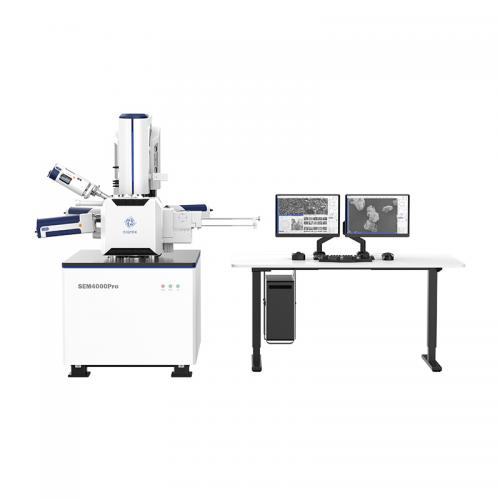
Analytical Schottky Field Emission Scanning Electron Microscope (FESEM) CIQTEK SEM4000Pro is an analytical FE-SEM model equipped with a high-brightness and long-life Schottky field emission electron gun. Its three-stage electromagnetic lens design offers significant advantages in analytical applications such as EDS / EDX, EBSD, WDS, and more. The model comes standard with a low-vacuum mode and a high-performance low-vacuum secondary electron detector, as well as a retractable backscattered electron detector, which benefits the observation of poorly conductive or non-conductive specimens. Contact our U.S. team: info.usa@ciqtek.com
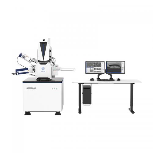
CIQTEK SEM5000 is a field emission scanning electron microscope(FESEM) with high-resolution imaging and analysis ability, supported by abundant functions, benefits from advanced electron optics column design, with high-pressure electron beam tunnel technology (SuperTunnel), low aberration, and non-immersion objective lens, achieves low voltage high-resolution imaging, the magnetic specimen can also be analyzed. With optical navigation, automated functionalities, carefully designed human-computer interaction user interface, and optimized operation and use process, no matter if you are an expert or not, you can quickly get started and complete high-resolution imaging and analysis work.
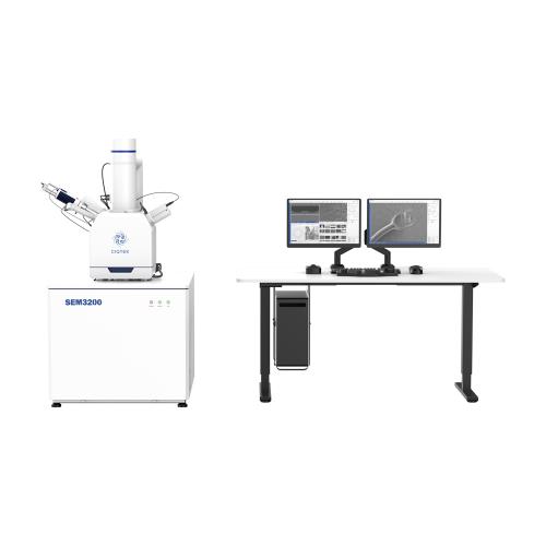
High-Performance and Universal Tungsten Filament SEM Microscope The CIQTEK SEM3200 SEM Microscope is an excellent general-purpose Tungsten Filament Scanning Electron Microscope (SEM) with outstanding overall capabilities. Its unique Dual-anode electron gun structure ensures high resolution and improves image signal-to-noise ratio at low excitation voltages. Furthermore, it offers a wide range of optional accessories, making the SEM3200 a versatile analytical instrument with excellent expandability. Contact our U.S. team: info.usa@ciqtek.com
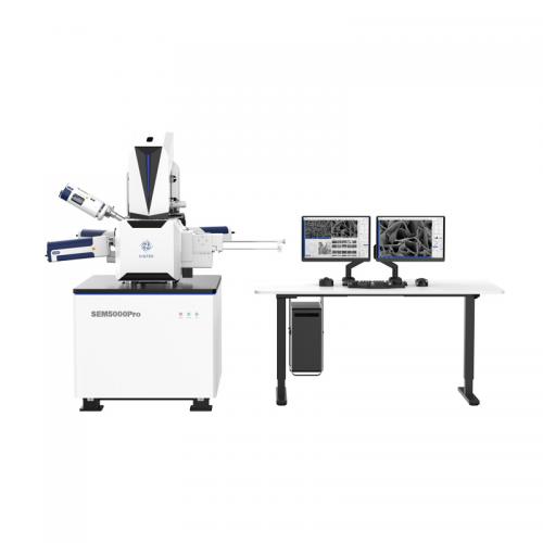
Ultra-High Resolution Schottky Field Emission Scanning Electron Microscope The SEM5000Pro (G2) field-emission scanning electron microscope is designed for stability, reliability, ease of use, and productivity, bringing field-emission imaging capabilities to a wide range of laboratories. Combining ultra-high spatial resolution with long-term operating stability, it consistently delivers high-quality images for applications ranging from advanced nanomaterials characterization to semiconductor R&D and manufacturing, meeting the demanding needs of research institutions and industrial quality-control laboratories.
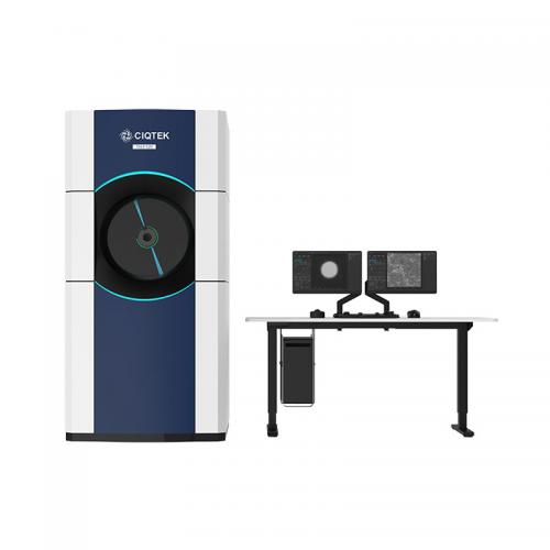
120kV Field Emission Transmission Electron Microscope (TEM) 1. Divided Workspaces: Users operate TEM in a divided room with comfort reducing environmental interference to TEM. 2. High Operational Efficiency: Designated software integrates highly automated processes, allowing efficient TEM interaction with real-time monitoring. 3. Upgraded Operational Experience: Equipped with a field emission electron gun with a highly automated system. 4. High Expandability: There are sufficient interfaces reserved for users to upgrade to a higher configuration, which meets diverse application requirements.
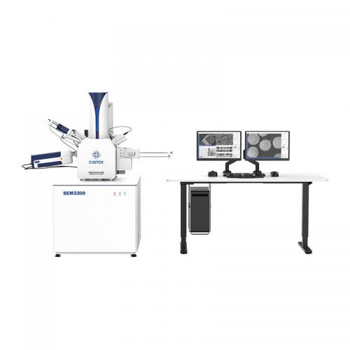
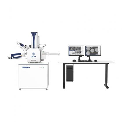
Ultra High-Resolution Tungsten Filament Scanning Electron Microscope The CIQTEK SEM3300 Scanning Electron Microscope (SEM) incorporates technologies such as "Super-Tunnel" electron optics, inlens electron detectors, and electrostatic & electromagnetic compound objective lens. By applying these technologies to the tungsten filament microscope, the long-standing resolution limit of such SEM is surpassed, enabling the tungsten filament SEM to perform low-voltage analysis tasks previously only achievable with field emission SEMs.
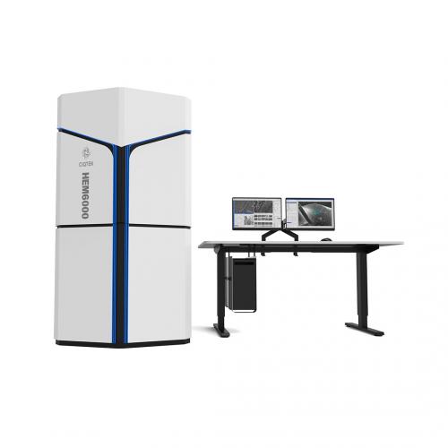
High-speed Fully Automated Field Emission Scanning Electron Microscope Workstation CIQTEK HEM6000 facilities technologies such as the high-brightness large-beam current electron gun, high-speed electron beam deflection system, high-voltage sample stage deceleration, dynamic optical axis, and immersion electromagnetic & electrostatic combo objective lens to achieve high-speed image acquisition whilst ensuring nano-scale resolution. The automated operation process is designed for applications such as a more efficient and smarter large-area high-resolution imaging workflow. Its imaging speed is over five times faster than that of a conventional field emission scanning electron microscope (FESEM).
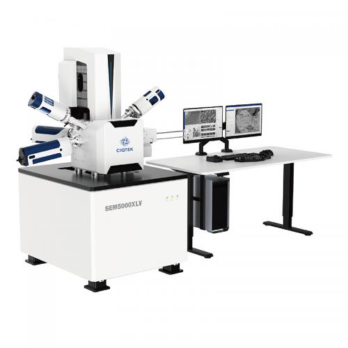
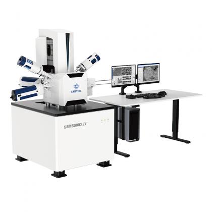
Analytical Schottky Field Emission Scanning Electron Microscopy (FESEM) The SEM5000XLV combines high-resolution imaging with high-current analytical capability and supports rapid switching between low-vacuum and high-current operating modes. It supports integration with optional EDS and EBSD modules, providing efficient characterization of challenging specimens and a comprehensive solution for localized microstructural and compositional analysis. Contact our U.S. team: info.usa@ciqtek.com
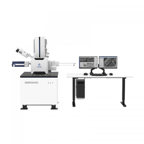
High-Performance and Multi-Purpose Field Emission Scanning Electron Microscope The SEM4000X (G2) is an ideal FE-SEM for microscale analysis and inspection. Combining stable, user-friendly operation with a multi-detector system and beam-deceleration capabilities, it delivers high-resolution imaging at low landing voltages. Balancing performance, reliability, and total cost of ownership, it provides a dependable solution for modern materials-analysis laboratories.