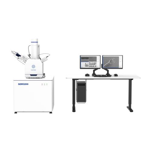
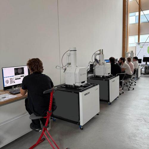
High-Performance and Multi-Purpose Field Emission Scanning Electron Microscope
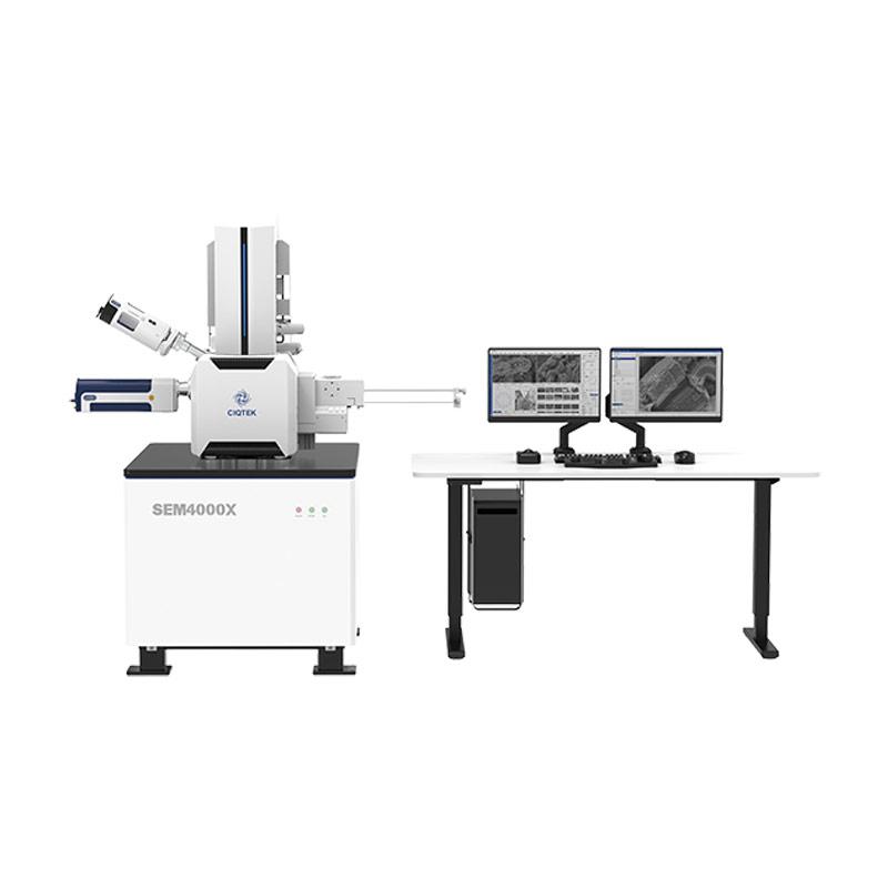
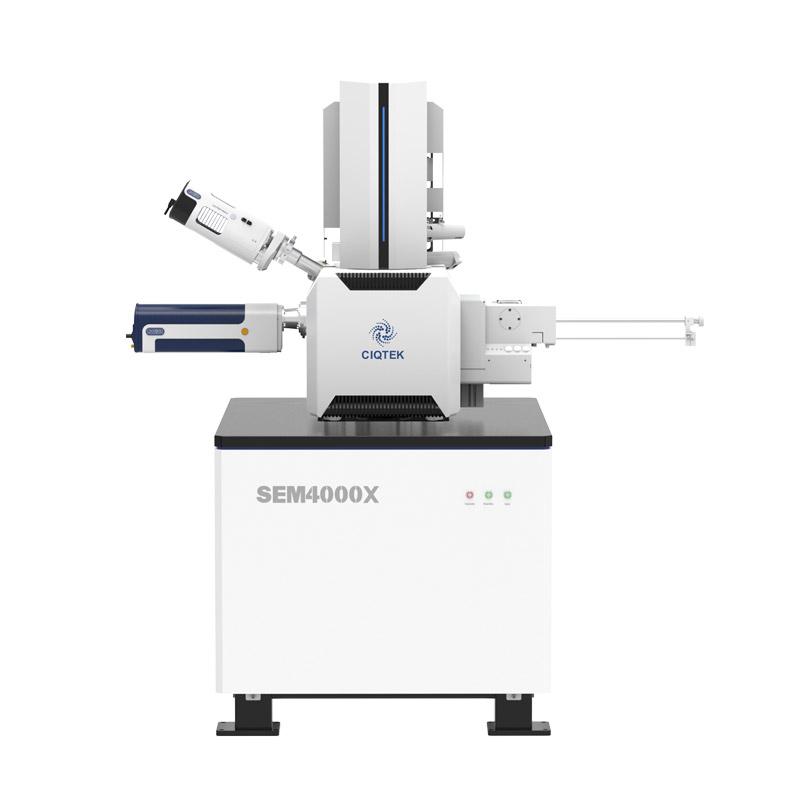
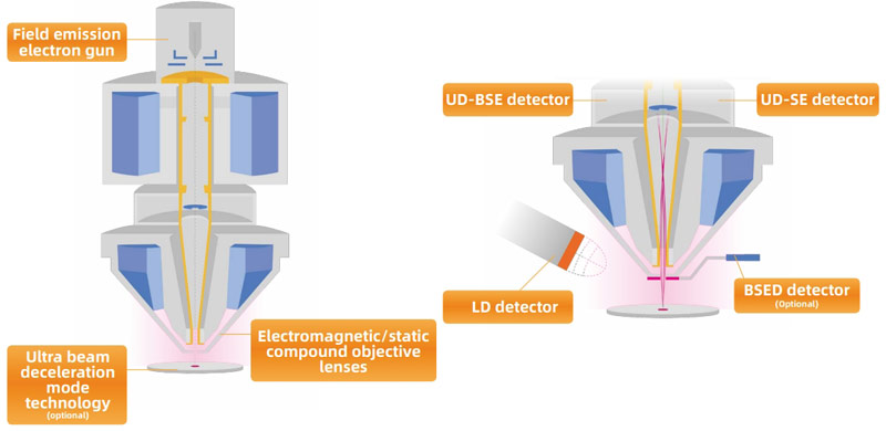
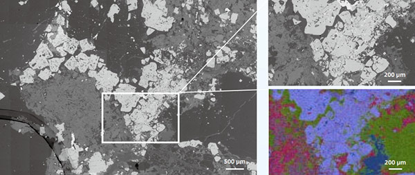
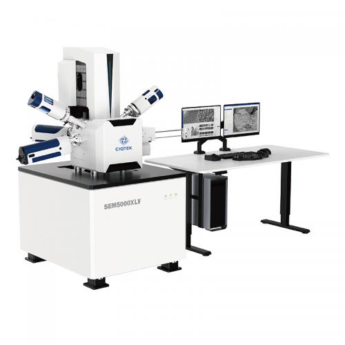
The SEM4000X (G2) is an ideal FE-SEM for microscale analysis and inspection. Combining stable, user-friendly operation with a multi-detector system and beam-deceleration capabilities, it delivers high-resolution imaging at low landing voltages. Balancing performance, reliability, and total cost of ownership, it provides a dependable solution for modern materials-analysis laboratories.


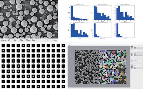
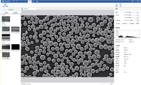
The CIQTEK SEM Microscope software employs various target detection and segmentation algorithms, suitable for different types of particle and pore samples. it enables quantitative analysis of particle and pore statistics and can be applied in fields such as materials science, geology, and environmental science.

Perform online or offline image post-processing on images captured by electron microscopes and integrate commonly used EM image processing functions, convenient measurement, and annotation tools.

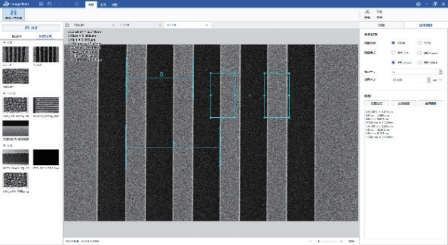
Automatic recognition of line width edges, resulting in more accurate measurements and higher consistency. Support multiple edge detection modes, such as Line, Space, Pitch, etc. Compatible with multiple image formats and equipped with various commonly used image post-processing functions. The software is easy to use, efficient, and accurate.

Provide a set of interfaces for controlling the SEM microscope, including image acquisition, operating condition settings, power on/off, stage control, etc. Concise interface definitions allow for the rapid development of specific electron microscope operation scripts and software, enabling automated tracking of regions of interest, industrial automation data acquisition, image drift correction, and other functions. Can be used for software development in specialized areas such as diatom analysis, steel impurity inspection, cleanliness analysis, raw material control, etc.

| CIQTEK SEM4000X FESEM Microscope Specifications | ||
| Electron Optics | Resolution | 0.9 nm @ 30 kV, SE 1.0 nm @15 kV, SE 1.8 nm @1 kV, SE 1.5 nm @1 kV (Ultra beam deceleration) 0.8 nm @15 kV (Ultra beam deceleration) |
| Acceleration Voltage | 0.2 kV ~ 30 kV | |
| Magnification (Polaroid) | 1 ~ 1,000,000 x | |
| Electron Gun Type | Schottky Field Emission Electron Gun | |
| Specimen Chamber | Camera | Dual Cameras (Optical navigation + chamber monitoring) |
| Stage Range |
X: 110 mm Y: 110 mm Z: 65 mm T: -10°~ +70° R: 360° |
|
| SEM Detectors and Extensions | Standard |
In-lens Electron Detector: UD-BSE/UD-SE Everhart-Thornley Detector: LD |
| Optional |
Backscattered Electron Detector (BSED) Retractable Scanning Transmission Electron Microscopy Detector (STEM) Low Vacuum Detector (LVD) Energy Dispersive Spectrometer (EDS / EDX) Electron Backscatter Diffraction Pattern (EBSD) Specimen Exchange Loadlock (4 inch /8 inch) Trackball & Knob Control Panel Ultra Beam Deceleration Mode Technology |
|
| User Interface | Language | English |
| OS | Windows | |
| Navigation | Optical Navigation, Gesture Quick Navigation, Trackball (optional) | |
| Automatic Functions | Auto Brightness & Contrast, Auto Focus, Auto Stigmator | |