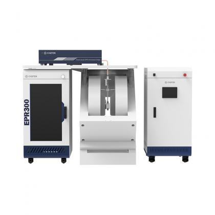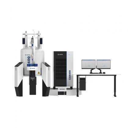



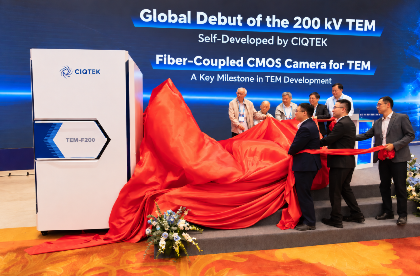
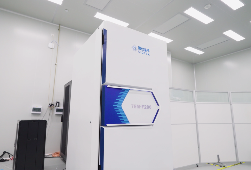
CIQTEK has officially launched its 200 kV field emission transmission electron microscope, TEM-F200, delivering 0.10 nm information resolution and featuring several key subsystems developed in-house.
Unveiled on October 18 at the 2026 National Electron Microscopy Annual Conference in China, the TEM-F200 is designed for demanding work in materials science, semiconductor research, and nanoscale characterization. The launch also marks another step toward a more complete domestic TEM platform, from key hardware to imaging and analysis workflows.
Built Around Resolution, Stability, and Practical Use
For TEM users, resolution is only part of the story. Stability, ease of operation, detector performance, automation, and service all affect what the microscope can actually deliver day-to-day.
The TEM-F200 combines a 200 kV field emission electron source with a self-developed high-voltage power supply and optical system.
A thermostatic water-cooled objective lens and four-axis sample stage help support stable imaging, while automated aperture control, position memory, and one-click adjustment are designed to reduce repetitive manual work.
The main imaging camera is CIQTEK’s self-developed 16-megapixel fiber-coupled CMOS camera, built specifically for TEM use. The camera combines a 9 μm CMOS sensor, 4K × 4K imaging, and up to 24 fps at full resolution.
Less Time at the Controls, More Time on the Sample
The TEM-F200 also puts a strong focus on workflow.
Fluorescent-screen images can be transferred directly to the PC display, while high-voltage control, electron-gun auto-start, vacuum operation, sample-position auto navigation, and STEM detector movement can all be integrated into the system workflow.
For laboratories that need more flexibility, the platform can also be expanded with EDS, EELS, 4D-STEM, 3D electron diffraction, side cameras, cryogenic components, and in situ holders.
From FinFET Devices to Advanced Alloys
The new system has already been demonstrated on a range of demanding samples.
For semiconductor FinFET devices, local nanoscale features and fine lattice structures were clearly resolved, with FFT analysis showing a spacing down to 1.045 Å.
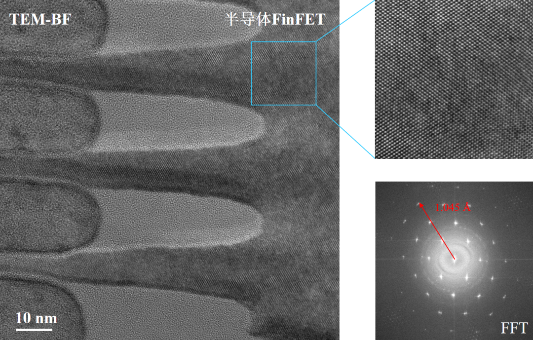
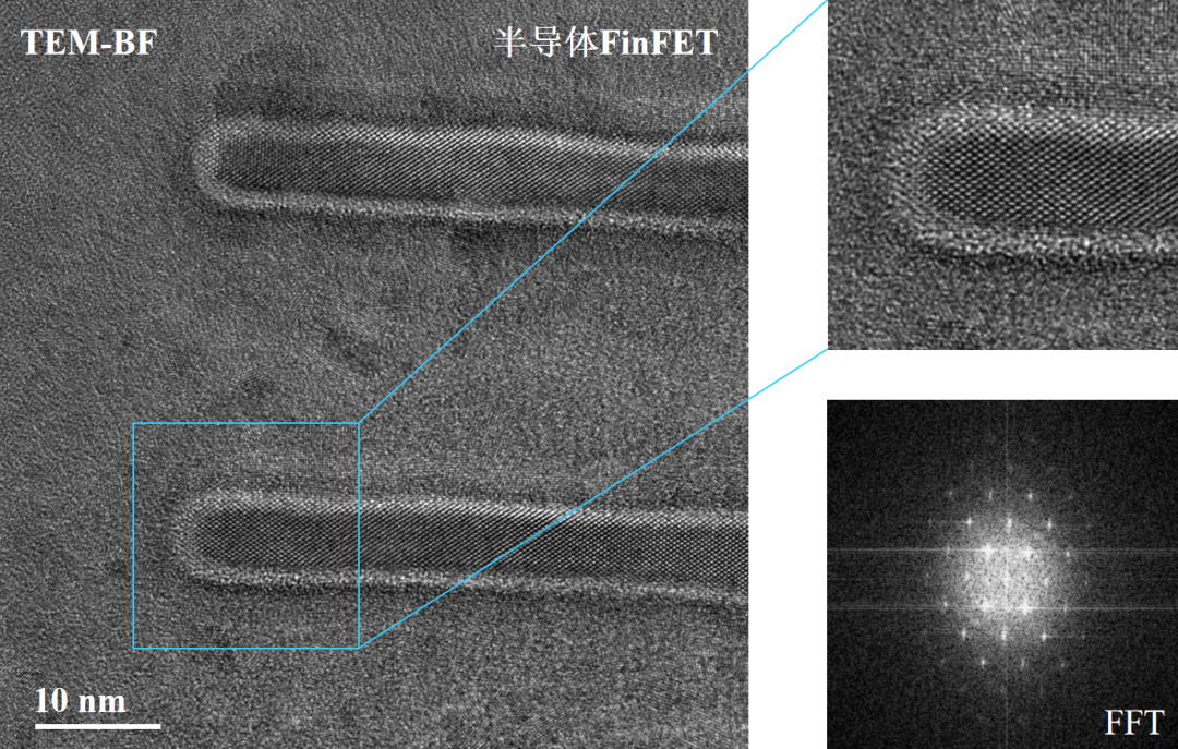
Semiconductor FinFET
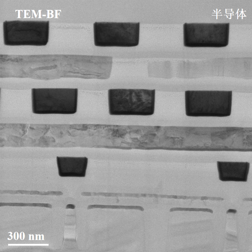
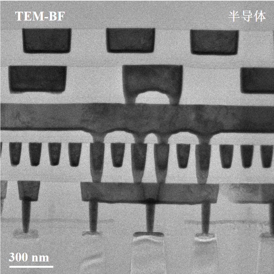
Cross-sectional imaging of semiconductor memory chips clearly revealed multilayer thin-film and dielectric structures.
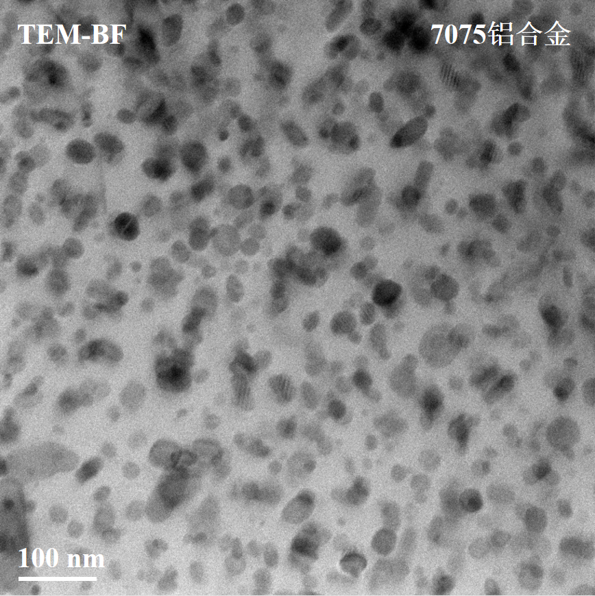
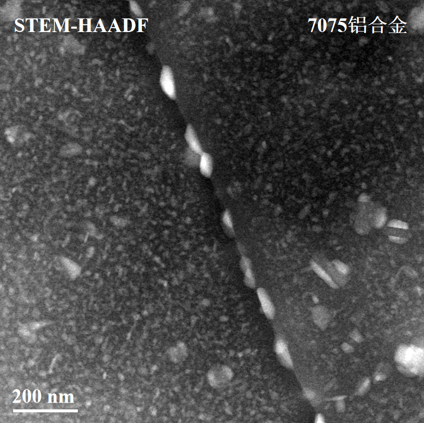
For 7075 aerospace aluminum alloy, TEM-BF and STEM-HAADF imaging resolved nanoscale precipitates, discontinuous grain-boundary phases, and precipitate-free zones.
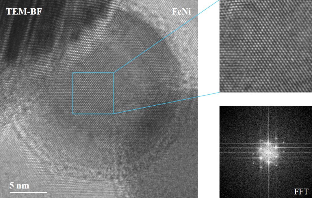
The system was also used to examine FeNi nanometer-scale particles, where the particles appeared nearly spherical and showed a visible amorphous outer layer.
Expanding the TEM Platform from 120 kV to 200 kV
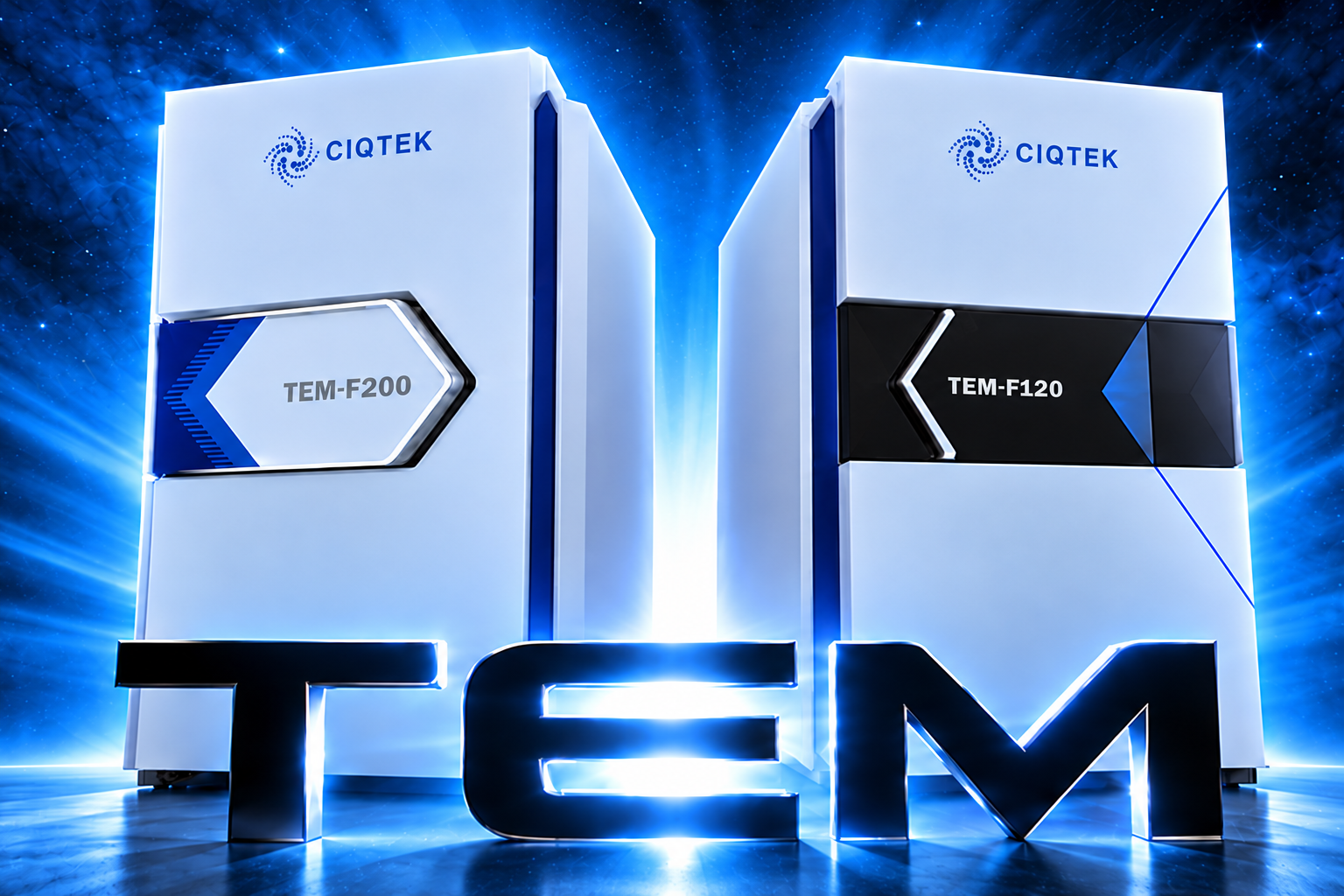
Alongside the TEM-F200, CIQTEK also introduced the 120 kV TEM-F120, equipped with a Schottky field emission electron gun.
The TEM-F120 is aimed at laboratories that need a balance of resolution, usability, and a smaller operating footprint, including research in life science, routine materials analysis, and general microscopy applications.
Together, the TEM-F120 and TEM-F200 expand CIQTEK’s TEM portfolio from 120 kV to 200 kV, covering a broader range of research needs.
For researchers working in semiconductors, materials science, nanotechnology, and other fields where nanoscale structure matters, the TEM-F200 is designed to make high-resolution TEM work more accessible, more integrated, and easier to bring into daily laboratory use.