Products

Products

CIQTEK is the manufacturer and global supplier of high-performance scientific instruments, such as Electron Microscopes, Electron Paramagnetic Resonance (Electron Spin Resonance), Gas Adsorption Analyzers, Scanning NV Microscopes, etc.
Applications
Study of Skyrmion - Quantum Diamond NV-center AFM Applications
Can you imagine a laptop hard drive the size of a grain of rice? Skyrmion, a mysterious quasiparticle structure in the magnetic field, could make this seemingly unthinkable idea a reality, with more storage space and faster data transfer rates for this "grain of rice. So how to observe this strange particle structure? The CIQTEK Quantum Diamond Atomic Force Microscope (QDAFM), based on the nitrogen-vacancy (NV) center in diamond and AFM scanning imaging, can tell you the answer.     What is Skyrmion   With the rapid development of large-scale integrated circuits, the chip process into the nanometer scale, the quantum effect is gradually highlighted, and "Moore's Law" encountered physical limits. At the same time, with such a high density of integrated electronic components on the chip, the thermal dissipation problem has become a huge challenge. People urgently need a new technology to break through the bottleneck and promote the sustainable development of integrated circuits.   Spintronics devices can achieve higher efficiency in information storage, transfer, and processing by exploiting the spin properties of electrons, which is an important way to break through the above dilemma. In recent years, topological properties in magnetic structures and their related applications are expected to be the information carriers of next-generation spintronic devices, which is one of the current research hotspots in this field.   The skyrmion (hereafter referred to as a magnetic skyrmion) is a topologically protected spin structure with quasiparticle properties, and as a special kind of magnetic domain wall, its structure is a magnetization distribution with vortices. Similar to the magnetic domain wall, there is also a magnetic moment flip in the skyrmion, but unlike the domain wall, the skyrmion is a vortex structure, and its magnetic moment flip is from the center outward, and the common ones are Bloch-type skyrmions and Neel-type skyrmions.   Figure 1: Schematic diagram of the structure of skyrmion. (a) Neel-type skyrmions (b) Bloch-type skyrmions   The skyrmion is a natural information carrier with superior properties such as easy manipulation, easy stability, small size, and fast driving speed. Therefore, the electronic devices based on skyrmions are expected to meet the performance requirements for future devices in terms of non-volatile, high capacity, high speed, and low power consumption.   What are the Applications of Skyrmions   Skyrmion Racetrack Memory Racetrack memory uses magnetic nanowires as tracks and magnetic domain walls as carriers, with electric current driving the motion of the magnetic domain walls. In 2013, the researchers proposed the skyrmion racetrack memory, which is a more promising alternative. Compared to the drive current density of a magnetic domain wall, the skyrmion is 5-6 orders of magnitude smaller, which can lead to lower energy consumption and heat generation. By comp...
Diamond NV-center Magnetic Imaging Technology for Cell Research
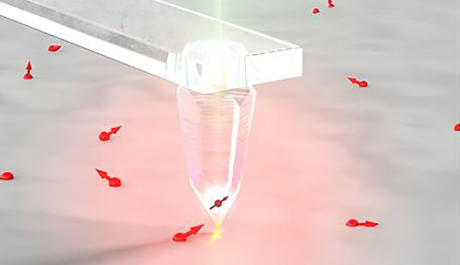
Light, electricity, heat, and magnetism are all important physical quantities involved in life science measurements, with optical imaging being the most widely used. With the continuous development of technology, optical imaging, especially fluorescence imaging, has greatly expanded the horizon of biomedical research. However, optical imaging is often limited by the background signal in biological samples, the instability of fluorescence signal, and the difficulty of absolute quantification, which to some extent restrict its application. Magnetic resonance imaging (MRI) is a good alternative and has a wide range of applications in some important life science scenarios, such as the examination of cranial, neurological, muscle, tendon, joint, and abdominopelvic organ lesions, due to its penetrating, low background and stability characteristics. Although MRI is expected to address the above-mentioned shortcomings of optical imaging, it is limited by low sensitivity and low spatial resolution, making it difficult to apply to imaging at the tissue level with micron to nanometer resolution.    An emerging quantum magnetic sensor developed in recent years, the nitrogen-vacancy (NV) center, a luminescent dot defect in diamond, NV center-based magnetic imaging technology enables the detection of weak magnetic signals with resolution up to the nanometer level and is non-invasive. This provides a flexible and highly compatible magnetic field measurement platform for the life sciences. It is unique for conducting tissue-level studies and clinical diagnostics in the fields of immunity and inflammation, neurodegenerative diseases, cardiovascular diseases, biomagnetic sensing, magnetic resonance contrast agents, and especially for biological tissues containing optical backgrounds, and optical transmission aberrations, and requires quantitative analysis.     Diamond NV-center Magnetic Imaging Technology   There are two main types of diamond NV-center magnetic imaging technology: scanning magnetic imaging and wide-field magnetic imaging. Scanning magnetic imaging is combined with the atomic force microscopy (AFM) technique, which uses a diamond single-color center sensor. The imaging method is a single-point scanning type of imaging, which has a very high spatial resolution and sensitivity. However, the imaging speed and imaging range limit the application of this technique in some areas. Wide-field magnetic imaging, on the other hand, uses a tethered diamond sensor with a high concentration of NV centers compared to a single NV center, which has reduced spatial resolution but shows great potential for wide-field, real-time imaging. The latter may be more appropriate for research in the field of cellular magnetic imaging.   Applications of  NV center Wide-field Magnetic Imaging Technology in Cell Research   Application 1: Magnetic imaging of magnetotactic bacteria   The magnetotactic bacterium is a class of bacter...
New Horizons for 2D Magnetic Materials - Quantum Diamond NV-center AFM Applications
For centuries, mankind has been exploring magnetism and its related phenomena without pause. In the early days of electromagnetism and quantum mechanics, it was difficult for humans to imagine the attraction of magnets to iron, and the ability of birds, fish, or insects to navigate between destinations thousands of miles apart - amazing and interesting phenomena with the same magnetic origin. These magnetic properties originate from the moving charge and spin of elementary particles, which are as prevalent as electrons.    Two-dimensional magnetic materials have become a research hotspot of great interest, and they open up new directions for the development of spintronics devices, which have important applications in new optoelectronic devices and spintronics devices. Recently, Physics Letters 2021, No. 12, also launched a special feature on 2D magnetic materials, describing the progress of 2D magnetic materials in theory and experiments from different perspectives.    A two-dimensional magnetic material only a few atoms thick can provide the substrate for very small silicon electronics. This amazing material is made of pairs of ultra-thin layers that are stacked together by van der Waals forces, i.e. intermolecular forces, while the atoms within the layers are connected by chemical bonds. Although only atomically thick, it still retains physical and chemical properties in terms of magnetism, electricity, mechanics, and optics.     Two-dimensional Magnetic Materials Image referenced from https://phys.org/news/2018-10-flexy-flat-functional-magnets.html   To use an interesting analogy, each electron in a two-dimensional magnetic material is like a tiny compass with a north and south pole, and the direction of these "compass needles" determines the magnetization intensity. When these infinitesimal "compass needles" are spontaneously aligned, the magnetic sequence constitutes the fundamental phase of matter, thus allowing the preparation of many functional devices, such as generators and motors, magnetoresistive memories, and optical barriers. This amazing property has also made two-dimensional magnetic materials hot. Although integrated circuit manufacturing processes are now improving, they are already limited by quantum effects as devices are shrinking. The microelectronics industry has encountered bottlenecks such as low reliability and high power consumption, and Moore's law, which has lasted for nearly 50 years, has also encountered difficulties (Moore's law: the number of transistors that can be accommodated on an integrated circuit double in about every 18 months). If two-dimensional magnetic materials can be used in the future in the field of magnetic sensors, random memory, and other new spintronics devices, it may be possible to break the bottleneck of integrated circuit performance.    We already know that magnetic van der Waals crystals carry special magnetoelectric effects, and therefore quan...
Learn More
Leave A Message
Submit
Top

Leave A Message

Leave A Message
Please feel free to contact us for more details, request a quote or book an online demo! We will reply you as soon as we can.
Submit

Home

Products

Chat

contact