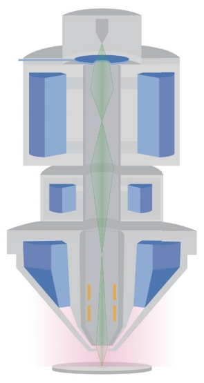
▶ Dual-Anode Structure at Electron Gun *Optional
Intermittent Anode
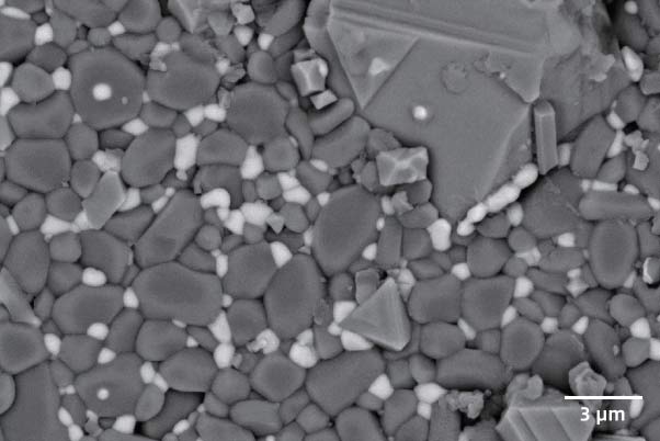
The intermittent anode is set up in between the cathode assembly and the anode. Under low excitation voltage, the extraction efficiency of the electron beam can be improved, the resolution can be increased by 10%, and the signal-to-noise ratio can be increased by 30%.
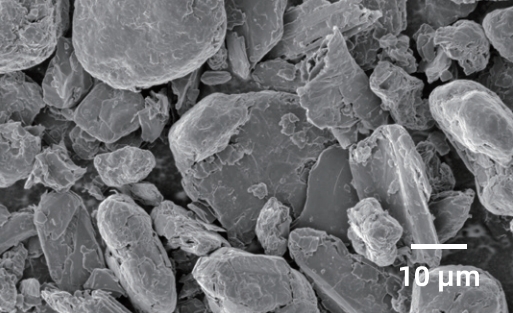
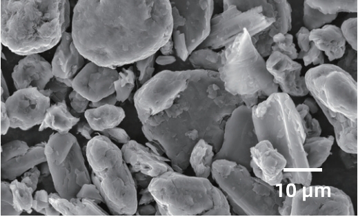
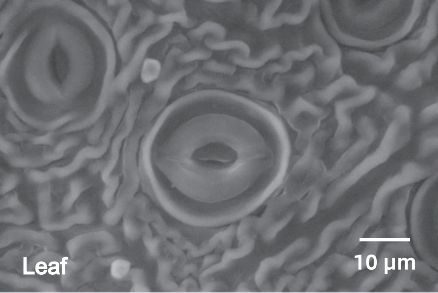
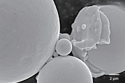
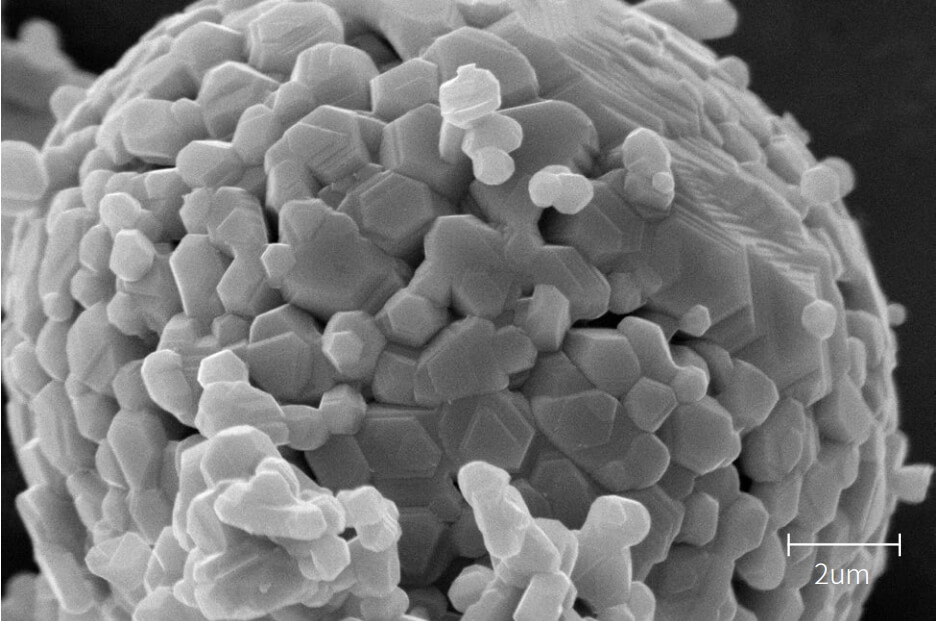
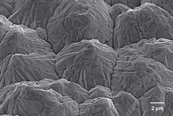
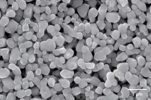
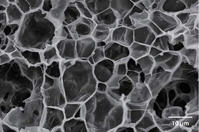
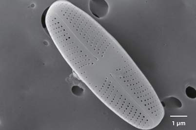
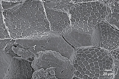
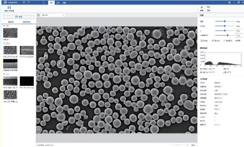
For carbon material samples, under low excitation voltages, the beam penetration depth is shallow, enabling the capturing of the true surface morphology information with richer details of the specimen.
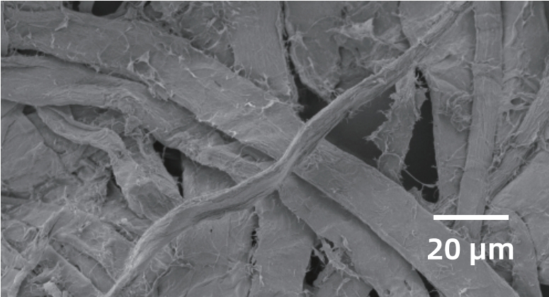
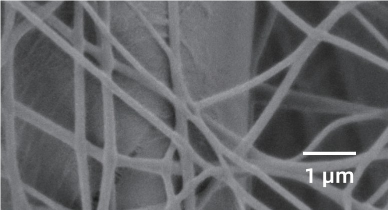
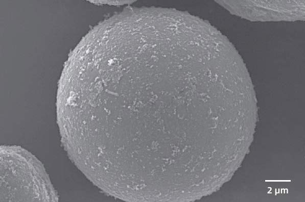
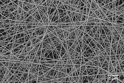
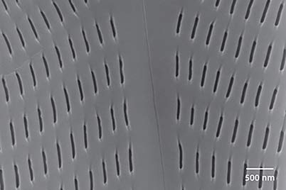
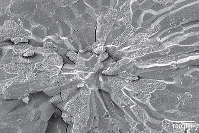
For polymer fiber samples, high excitation voltages cause beam damage to the specimen, while low voltage beam enables the preservation of surface details without damage.
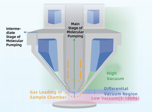
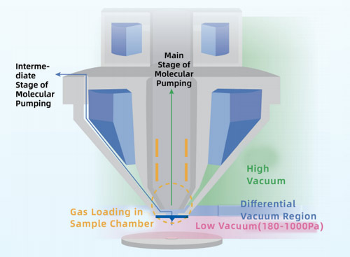
▶ Low Vacuum SEM Mode
The CIQTEK SEM3200 SEM Microscope supports 2-stage low vacuum modes: 5~180 Pa chamber pressure can be reached without pressure limiting aperture, and 180~1000 Pa is achievable with PLA. The specially designed objective lens vacuum chamber minimizes electron mean free path in low-vacuum, and maintains the resolution at 3 nm @ 30 kV.
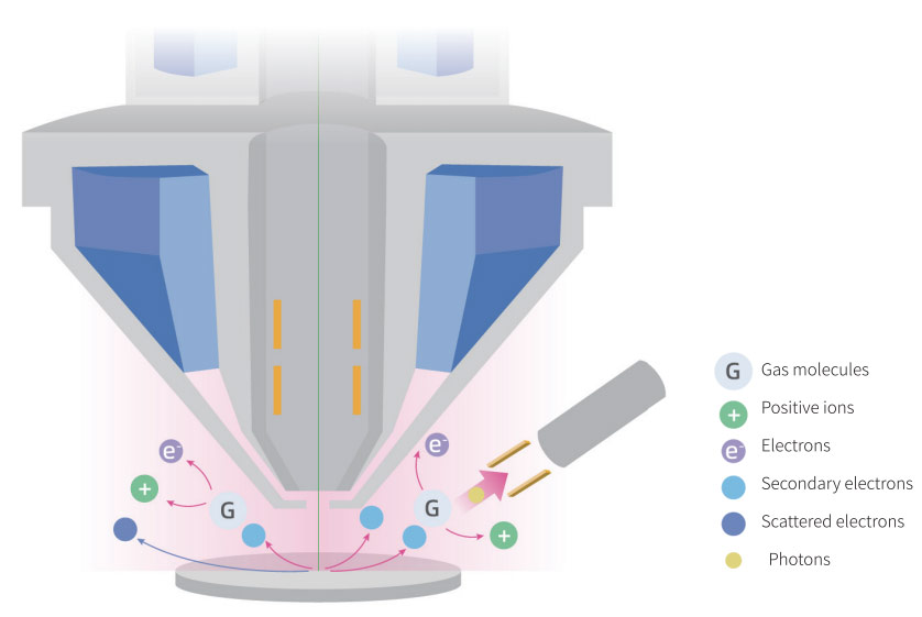
The incident electron beam ionizes the air molecules on top of the surface, producing electrons and ions, in which ions neutralize the charged particles generated on the sample surface, achieving the effect of charge mitigation.
The secondary electron emission from the sample surface ionizes air molecules, generating electrons, ions, and photo signals simultaneously. The generated electrons then ionize other air molecules and a large number of photo signals are produced and then captured by a Low Vacuum Detector (LVD).
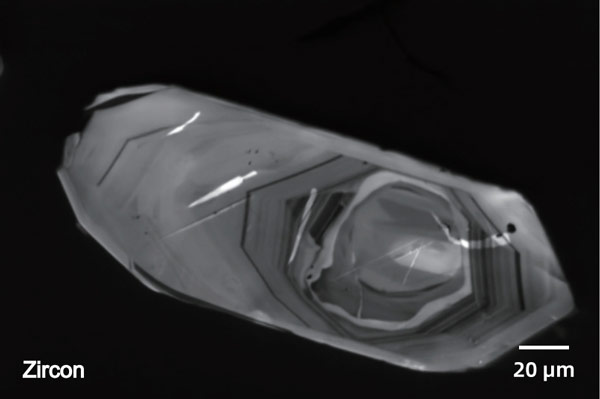
In high vacuum mode, LVD directly detects the cathodoluminescence signal emitted from the specimen, which can be captured for cathodoluminescence imaging, with simultaneous imaging from the BSED channel.
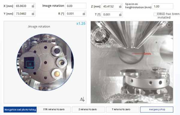
▶ Optical Navigation
Using a vertically mounted chamber camera to capture optical images for specimen stage navigation allows for a more intuitive and accurate specimen positioning.
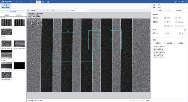
▶Intelligent Assisted Image Astigmatism Correction
Under this mode, the astigmatism value of X and Y varies with the pixels. The image clarity is maximized at the optimal astigmatism value, enabling rapid stigmator adjustment.
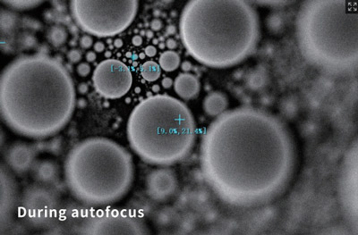
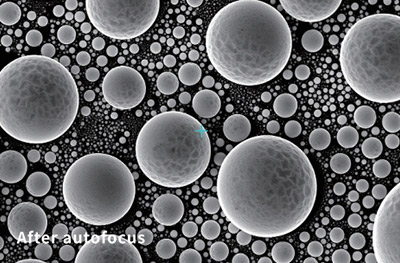
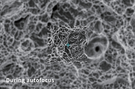
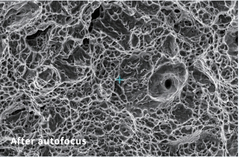
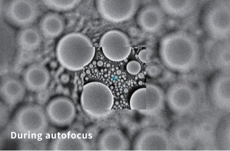
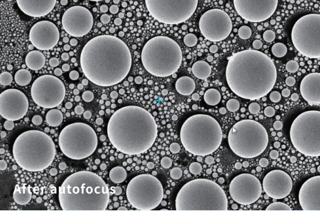
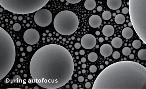
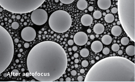
▶ Auto Functions
Improved Automatic Brightness & Contrast, Automatic Focus, and Automatic Astigmatism Correction Functions. Imaging by a single click!
>> Automatic Focus
>> Automatic Astigmatism Correction
>> Automatic Brightness & Contrast
▶ Safer to Use
▶ Easy Filament Replacement
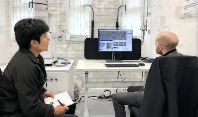
Pre-aligned replacement filament module ready to use.