Products

Products

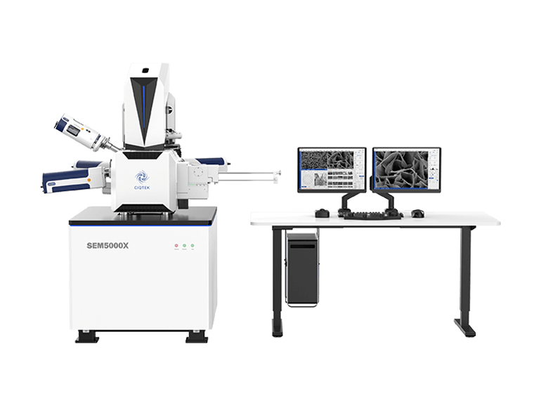
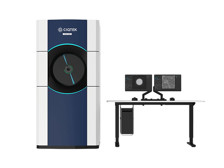
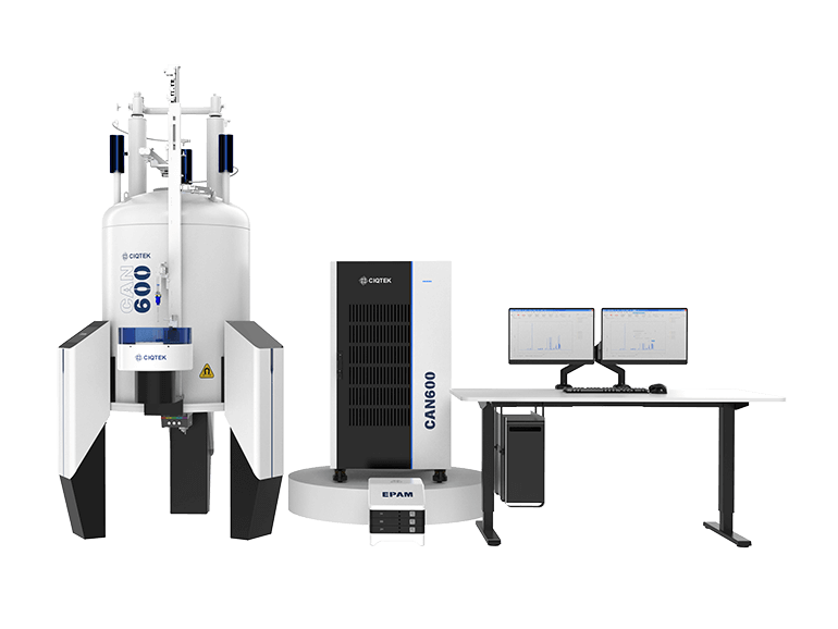
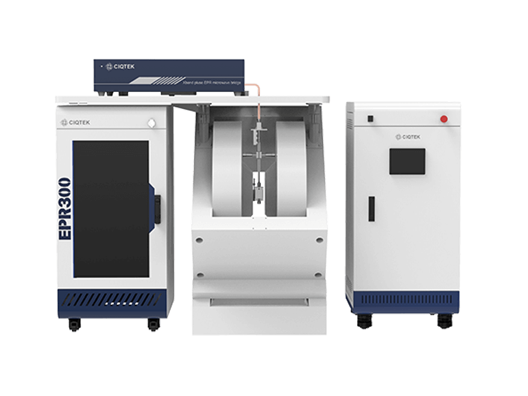
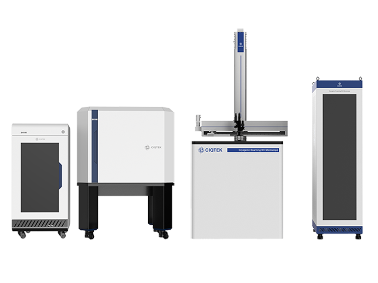
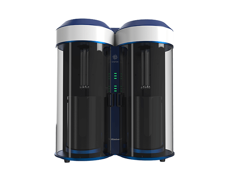
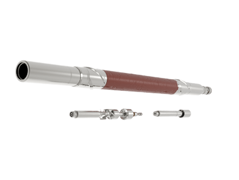
CIQTEK is the manufacturer and global supplier of high-value scientific instruments, such as Scanning Electron Microscopes (SEMs), Electron Paramagnetic Resonance (Electron Spin Resonance) Spectroscopy, Scanning NV Probe Microscope, Gas Adsorption Analyzer, etc.
Learn More
Leave A Message
Submit
Applications
CIQTEK Scanning Electron Microscope Facilitates Quality Improvement of
CIQTEK Scanning Electron Microscope Facilitates Quality Improvement of "Super Nanocoating"
Introducing CIQTEK tungsten filament Scanning Electron Microscope SEM3200 provides researchers with clear nanoscale images, allowing them to examine the microstructure and morphology of the coating layers visually. Additionally, the equipped Energy Dispersive Spectrometer (EDS) enables precise analysis of material composition and element distribution, effectively guiding process optimization in research and development. - Dr. Zhang, Head of Major Customers/Quality Director Coating: Giving Products a "Super Nanocoating"   The development of coating technology not only showcases the depth of materials science but also demonstrates the precision manufacturing processes. Dr. Zhang explains, "Our company has developed superior-performing coatings such as diamond-like carbon (DLC)/ titanium-aluminum-carbon (TAC) films, nitride films, carbide films, high-density metal/alloy films, and optical films. These coating layers are like giving products a 'super nanocoating'."     CIQTEK Scanning Electron Microscope Enhances the Quality of Nanocoating Layers   Dr. Zhang states, "With the SEM3200, we can readily detect the total thickness of the coating layers, as well as the thickness and composition of each designed layer (substrate layer, transition layer, surface layer) in the samples provided by customers. Our in-house research and development can quickly provide design solutions. This enhances the efficiency of coating process development."   The SEM3200 plays a crucial role in research and development and also acts as a key tool in quality control. "We can use it for failure analysis," says Dr. Zhang."Through comprehensive testing and characterization, we can identify the root causes of defective products, continuously improving product quality and yield."   Scanning Electron Microscopes Facilitate the High-quality Development of Manufacture    Dr. Zhang expresses that the SEM3200 not only operates in good condition with a user-friendly interface and high automation but also receives prompt responses from the CIQTEK after-sales team, solving many practical problems. This not only reflects the outstanding performance of CIQTEK products but also demonstrates the significant role of high-end scientific instruments in supporting the development of high-tech enterprises.   In the future, CIQTEK will continue to provide first-class research solutions for more high-tech companies like coating, jointly promoting the flourishing development of the scientific and technological industry.
Electron Paramagnetic Resonance (EPR) technology offers solutions for water treatment research
The main pollutants in water bodies include pharmaceuticals, surfactants, personal care products, synthetic dyes, pesticides, and industrial chemicals. These pollutants are challenging to remove and can adversely affect human health, including the nervous, developmental, and reproductive systems. Therefore, protecting water environments is of utmost importance.   In recent years, advanced oxidation processes (AOPs) such as Fenton-like reactions, persulfate activation, and UV-light-induced AOPs (e.g., UV/Cl2, UV/NH2Cl, UV/H2O2, UV/PS) as well as photocatalysts (e.g., bismuth vanadate (BiVO4), bismuth tungstate (Bi2WO6), carbon nitride (C3N4), titanium dioxide (TiO2) have gained attention in the field of water treatment and environmental remediation.   These systems can generate highly reactive species such as hydroxyl radicals (•OH), sulfate radicals (•SO4-), superoxide radicals (•O2-), singlet oxygen (1O2), etc. These techniques significantly enhance the removal rates of organic pollutants compared to conventional physical and biological methods. The development of these water treatment technologies greatly benefits from the assistance of Electron Paramagnetic Resonance (EPR) technology.   CIQTEK offers the desktop Electron Paramagnetic Resonance spectrometer EPR200M and the X-band continuous-wave Electron Paramagnetic Resonance spectrometer EPR200-Plus, which provide solutions for studying photocatalysis and advanced oxidation processes in water treatment.   Application Solutions of Electron Paramagnetic Resonance (EPR) technology in water treatment research   - Detect, identify, and quantify reactive species such as •OH, •SO4-, •O2-, 1O2, and other active species generated in photocatalytic and AOPs systems.   - Detect and quantify vacancies/defects in remediation materials, such as oxygen vacancies, nitrogen vacancies, sulfur vacancies, etc.   - Detect doped transition metals in catalytic materials.   - Verify the feasibility and assist in optimizing various parameters of water treatment processes.   - Detect and determine the proportion of reactive species during water treatment processes, providing direct evidence for pollutant degradation mechanisms.     Application Cases of Electron Paramagnetic Resonance (EPR) technology in water treatment research   Case 1: EPR in UV/ClO2-based advanced oxidation technology   - EPR study of the degradation process of fluoroquinolone antibiotics in a UV-mediated AOPs system.   - Degradation of pharmaceuticals and personal care products (PPCPs) in water by chlorine dioxide under UV conditions.   - EPR detection and qualitative analysis of •OH and singlet oxygen as active species in the system.   - Increase in •OH and 1O2 concentrations with longer irradiation times, promoting antibiotic degradation.   - EPR detection of •OH and 1O2 co...
Application Cases |  The application of scanning electron microscope in metal fracture analysis
Application Cases | The application of scanning electron microscope in metal fracture analysis
What is a metal fracture? When a metal breaks under external forces, it leaves behind two matching surfaces called "fracture surfaces" or "fracture faces." The shape and appearance of these surfaces contain important information about the fracture process.   By observing and studying the morphology of the fracture surface, we can analyze the causes, properties, modes, and mechanisms of the fracture. It also provides insights into the stress conditions and crack propagation rates during the fracture. Similar to an "on-site" investigation, the fracture surface preserves the entire process of fracture. Therefore, examining and analyzing the fracture surface is a crucial step and method in studying metal fractures. Scanning electron microscope, with its large depth of field and high resolution, has been widely used in the field of fracture analysis.   The application of scanning electron microscope in metal fracture analysis   Metal fractures can occur in various failure modes. Based on the deformation level before fracture, they can be classified as brittle fracture, ductile fracture, or a mixture of both. Different fracture modes exhibit characteristic microscopic morphologies, and CIQTEK scanning electron microscope characterization can help researchers quickly analyze fracture surfaces.   Ductile fracture   Ductile fracture refers to the fracture that occurs after a significant amount of deformation in the component, and its main feature is the occurrence of obvious macroscopic plastic deformation. The macroscopic appearance is cup-cone or shear with a fibrous fracture surface, characterized by dimples. As shown in Figure 1, at the microscale, the fracture surface consists of small cup-shaped micropores called dimples. Dimples are microvoids formed by localized plastic deformation in the material. They nucleate, grow, and coalesce, eventually leading to fracture, and leaving traces on the fracture surface.   Figure 1: Ductile fracture surface of metal / 10kV / Inlens   Brittle fracture   Brittle fracture refers to the fracture that occurs without significant plastic deformation in the component. The material undergoes little or no plastic deformation before fracture. Macroscopically, it appears crystalline, and microscopically, it can exhibit intergranular fracture, cleavage fracture, or quasi-cleavage fracture. As shown in Figure 2, it is a mixed brittle-ductile fracture surface of metal. In the ductile fracture region, noticeable dimples can be observed. In the brittle fracture region, intergranular brittle fracture occurs along different crystallographic orientations. At the microscale, the fracture surface exhibits multiple facets of the grains, with clear grain boundaries and a three-dimensional appearance. Smooth and featureless morphology is often observed on the grain boundaries. When the grains are coarse, the fracture surface appears crystalline, also known as a crystalline fracture; when the...
Application Cases | Application of Field Emission SEM in Electrolytic Copper Foil
High-performance lithium copper foil is one of the key materials for lithium-ion batteries and is closely related to battery performance. With the increasing demand for higher capacity, higher density, and faster charging in electronic devices and new energy vehicles, the requirements for battery materials have also been raised. In order to achieve better battery performance, it is necessary to improve the overall technical indicators of lithium copper foil, including its surface quality, physical properties, stability, and uniformity.   Analysis of microstructure using scanning electron microscope-EBSD technique   In materials science, the composition and microstructure determine the mechanical properties. Scanning Electron Microscope (SEM) is a commonly used scientific instrument for the surface characterization of materials, allowing observation of the surface morphology of copper foil and the distribution of grains. In addition, Electron Backscatter Diffraction (EBSD) is a widely used characterization technique for analyzing the microstructure of metallic materials. By configuring an EBSD detector on a field-emission scanning electron microscope, researchers can establish the relationship between processing, microstructure, and mechanical properties.   The figure below shows the surface morphology of electrolytic copper foil captured by the CIQTEK Field-emission SEM5000   Copper Foil Smooth Surface/2kV/ETD Copper Foil Matte Surface/2kV/ETD When the sample surface is sufficiently flat, electron channel contrast imaging (ECCI) can be obtained using the SEM backscatter detector. The electron channeling effect refers to a significant reduction in the reflection of electrons from crystal lattice points when the incident electron beam satisfies the Bragg diffraction condition, allowing many electrons to penetrate the lattice and exhibit a "channeling" effect. Therefore, for polished flat polycrystalline materials, the intensity of backscatter electrons depends on the relative orientation between the incident electron beam and the crystal planes. Grains with larger misorientation will yield stronger backscattered electron signals and higher contrast, enabling the qualitative determination of grain orientation distribution through ECCI.   The advantage of ECCI lies in its ability to observe a larger area on the sample surface. Therefore, before EBSD acquisition, ECCI imaging can be used for rapid macroscopic characterization of the microstructure on the sample surface, including observation of grain size, crystallographic orientation, deformation zones, etc. Then, EBSD technology can be used to set the appropriate scanning area and step size for crystallographic orientation calibration in the regions of interest. The combination of EBSD and ECCI fully utilizes the advantages of crystallographic orientation imaging techniques in materials research.   By using ion beam cross-section polishing technology, CIQTEK obtain...
Application of Gas Adsorption Techniques in Characterizing Titanium Dioxide
Abstract: Titanium dioxide, widely known as titanium white, is an important white inorganic pigment extensively used in various industries such as coatings, plastics, rubber, papermaking, inks, and fibers. Studies have shown that the physical and chemical properties of titanium dioxide, such as photocatalytic performance, hiding power, and dispersibility, are closely related to its specific surface area and pore structure.   Using static gas adsorption techniques for precise characterization of parameters like specific surface area and pore size distribution of titanium dioxide can be employed to evaluate its quality and optimize its performance in specific applications, thereby further enhancing its effectiveness in various fields.   About Titanium Dioxide: Titanium dioxide is a vital white inorganic pigment primarily composed of titanium dioxide. Parameters such as color, particle size, specific surface area, dispersibility, and weather resistance determine the performance of titanium dioxide in different applications, with specific surface area being one of the key parameters. Specific surface area and pore size characterization help understand the dispersibility of titanium dioxide, thereby optimizing its performance in applications such as coatings and plastics. Titanium dioxide with a high specific surface area typically exhibits stronger hiding power and tinting strength.   In addition, research has indicated that when titanium dioxide is used as catalyst support, a larger pore size can enhance the dispersion of active components and improve the overall catalytic activity, while a smaller pore size increases the density of active sites, aiding in improving reaction efficiency. Hence, by regulating the pore structure of titanium dioxide, its performance as a catalyst support can be improved.   In summary, the characterization of specific surface area and pore size distribution not only aids in evaluating and optimizing the performance of titanium dioxide in various applications but also serves as an important means of quality control in the production process. Precise characterization of titanium dioxide enables a better understanding and utilization of its unique properties to meet the requirements in different application fields.   Application Examples of Gas Adsorption Techniques in Titanium Dioxide Characterization:   1. Characterization of Specific Surface Area and Pore Size Distribution of Titanium Dioxide for DeNOx Catalysts   Selective catalytic reduction (SCR) is one of the commonly applied and researched flue gas denitrification technologies. Catalysts play a crucial role in SCR technology, as their performance directly affects the efficiency of nitrogen oxide removal. Titanium dioxide serves as the carrier material for DeNOx catalysts, primarily providing mechanical support and erosion resistance to active components and catalytic additives, along with increasing the reaction surface area and pr...
Top

Leave A Message

Leave A Message
Please feel free to contact us for more details, request a quote or book an online demo! We will reply you as soon as we can.
Submit

Home

Products

Chat

contact