Product Center

Products

Science & Technology
Science and technology are areas of research and application involving systematic knowledge of the physical and natural world and the practical application of that knowledge. Science is concerned with understanding the fundamental principles and laws of the universe, and technology is concerned with the development and application of tools, machines and techniques to solve practical problems and improve human life.
Materials Science
Materials Science
Using advanced analytical instruments, study the interrelationship between the preparation or processing process of materials, the microstructure of materials, and the macroscopic properties of materials.
Chemicals
Chemicals
Analysis of the structure of substances containing unpaired electrons (such as isolated single atoms, conductors, magnetic molecules, transition metal ions, rare earth ions, ion clusters, doped materials, defective materials, biological radicals, metalloproteins, etc.) and their applications are realized by using wave spectroscopy.
Industrial & Applied Sciences
Provide high quality, high standard products & solutions for industrial users and applied scientific research based on advanced technology and reliable products.
Energy & Power
Energy & Power
Focus on the utilization of unconventional oil and gas resources such as shale oil and gas, coalbed methane, combustible ice, etc., and develop application scenarios such as downhole digital core analysis.
Biomedical & Life Science
Apply to resolve the structure and function of biological macromolecules, single-molecule imaging, subcellular imaging, cell sorting, and other fields, the measurement scale spans the nanometer to the micron scale.

About CIQTEK

CIQTEK is the global developer & manufacturer of high-precision scientific instruments. Our main business includes Electron Microscopes, Electron Paramagnetic Resonance (Electron Spin Resonance), Scanning NV Microscopes, and BET Surface Area & Pore Analyzer.
  • 0+
    Employees
  • 0% +
    Employees dedicated to R&D
  • 0+
    Patents pending or granted
News & Events

News

What's New
The world's first commercial low-temperature SNVM was released
Recently, the world's first commercial low-temperature Scanning Nitrogen-vacancy Probe Microscope (SNVM) was released in Hefei, Anhui, China. This instrument is mainly used to detect the surface magnetism of nanomaterials and will provide a new method for research in fields such as materials science, condensed matter physics, and life sciences. The instrument was independently developed by CIQTEK, marking a new breakthrough in the industrialization development of precision measurement technology.   Precision measurement refers to the use of properties such as energy level transitions, coherent superposition, and entanglement to achieve substantial improvements in measurement accuracy, sensitivity, resolution, etc.   The CIQTEK Scanning Nitrogen-vacancy Probe Microscope (SNVM) is an advanced scientific analytical instrument that combines diamond nitrogen-vacancy (NV) optical detected magnetic resonance (ODMR) technology and atomic force microscope (AFM) scanning imaging technology, which can realize quantitative and non-destructive magnetic imaging of magnetic samples with high spatial resolution and high sensitivity.   In addition to diamond NV color centers, there are many technical routes for precision measurement, including atomic magnetometers, atomic clocks, etc. Atomic magnetometer is a technology that uses the interaction between light and atoms to detect magnetic fields, which can detect coronary heart disease and abnormal heart rate. As a new generation of atomic clock, optical lattice clock can currently achieve an error of only 1 second in tens of billions of years. Each technical route shows its unique capabilities according to the application scenarios.     SNVM for Magnetic Imaging of BFO Films Precision sensors are known as "a key to the microscopic world." It is not only small, but also very sensitive. It can detect many signals that were undetectable and inaccurate in the past, such as brain magnetism and cardiac magnetism. It can be used for early diagnosis of neurological diseases, coronary heart disease and other diseases. At the same time, precision measurement has also brought about some innovations in detection methods, such as leakage current detection in lithium batteries in the new energy field, power grid management in the energy exploration field, and chip current imaging in the semiconductor/integrated circuit field.     SNVM for Imaging A Single Vortex Stray Magnetic Field The industry regards precision measurement as another "ripe industrialization" direction in the field of information technology, and technological innovation is becoming increasingly active. In recent years, many start-up companies in the field of measurement have been hatched around the world to explore various application scenarios and promote the progress of commercialization.     SNVM for Twisted Bilayer CrI3 Measurements Precision measurement is to change "invisible" to "visible"...
July 22, 2024
Introducing CIQTEK SEM3200: Unveiling the SEM Microscopy at Loughborough University, England
  The demo lab at Loughborough University is buzzing with excitement as we showcase the cutting-edge Scanning Electron Microscope SEM3200, a revolutionary addition to the UK market. In collaboration with the renowned Loughborough Materials Characterization Center (LMCC), SciMed is proud to introduce users to the new range of CIQTEK microscopes, backed by the world-leading expertise of the facility staff.   Loughborough University is no stranger to excellence. Ranked among the top 10 universities in the UK, it boasts a rich academic legacy and a commitment to scientific progress. Housed within the LMCC, an acclaimed state-of-the-art material analysis facility, the demo lab provides the perfect environment to unveil the SEM3200 and its exceptional capabilities.     Our journey began by collating images from various research groups closely affiliated with Loughborough University. We worked closely with these groups, enabling me to gather diverse samples for imaging. From micropatterned substrates produced through photolithography to the intricate surface of a microelectrode array, they have captured the essence of materials under the microscope. Furthermore, they have recently obtained a range of materials used in hydrogen energy cell technologies, expanding the possibilities of our imaging capabilities.     The feedback from the staff has been overwhelmingly positive. Universally, they have praised the user-friendly software interface, which allows for intuitive control within minutes of use. One standout feature is the eucentric 5-axis stage, which ensures impeccable focus and image position, even during significant changes in tilt angle. The SEM3200's modern design has truly impressed our users, as it effortlessly produces high-quality images with remarkable ease.     The SEM3200 represents a leap forward in microscopy technology, and its arrival at Loughborough University's demo lab is a cause for celebration. Researchers, scientists, and students alike can now access a microscope that combines world-class expertise with user-friendly operation, paving the way for groundbreaking discoveries and exceptional research outputs.   Step into the future of microscopy with the SEM3200. Experience the power of cutting-edge technology, supported by the top-tier infrastructure of Loughborough University's LMCC. Join us at the demo lab and witness firsthand the incredible potential of the SEM3200. Together, let's explore new frontiers and unlock a world of microscopic wonders.  
July 08, 2024
CIQTEK FIB-SEM Practical Demonstration - TEM Sample Preparation
FIB-SEM can be used for defect diagnosis, repair, ion implantation, in-situ processing, mask repair, etching, integrated circuit design modification, chip device production, and mask-less processing of large-scale integrated circuits. Nanostructure production, complex nanopattern processing, three-dimensional imaging and analysis of materials, ultra-sensitive surface analysis, surface modification, and transmission electron microscopy sample preparation, etc. It has a wide range of application requirements and is indispensable.   CIQTEK DB500 is a 
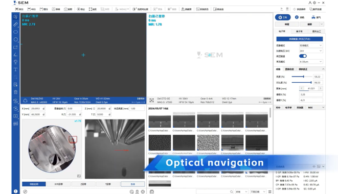
Field Emission Scanning Electron Microscope (FE-SEM) with a Focused Ion Beam (FIB) column for nano analysis and specimen preparation, which is applied with “SuperTunnel” electron optics technology, low aberration, and magnetic-free objective lens design, with low-voltage and high-resolution ability that ensures its nano-scale analytical capability. The ion column facilitates a Ga+ liquid metal ion source with a highly stable and high-quality ion beam to ensure nano-fabrication capability.   DB500 has an integrated nano-manipulator, gas injection system, electrical anti-contamination mechanism for the objective lens, and 24 expansion ports, making it an all-around nano-analysis and fabrication platform with comprehensive configurations and expandability.   In order to demonstrate the outstanding performance of DB500 to users, the Electron Microscopy team has specially planned the special program " CIQTEK FIB Show", which will present the wide range of applications in the fields of materials science, semiconductor industry, biomedicine, etc. in the form of video. The audience will understand the working principle of DB500, appreciate the stunning microscopic images it captures, and deeply explore the significance of this technology to scientific research and industrial development.   TEM sample preparation In this episode, we will show you how DB500 can prepare transmission electron microscope (TEM) samples efficiently and accurately.   As you can see from the video, DB500 prepares TEM samples with simple operation, few pre-processing steps, low learning costs, and efficient testing; it can achieve precise micro- and nanoscale cutting at fixed points, with controllable size and uniform thickness, and is suitable for a variety of microscopy and Microscopic spectroscopy analysis; and the integration of cutting, imaging, and analysis can be achieved.
July 04, 2024
Conferences & Exhibitions
CONTACT US

Contact

Top

Leave A Message

Leave A Message
Please feel free to contact us for more details, request a quote or book an online demo! We will reply you as soon as we can.
Submit

Home

Products

Chat

contact